- Thermal Management of Electronic Assemblies and Enclosures
Electronics Industry
Applications of CFD tools in PCB, Board-level and Chassis Level Thermal Simulations
Electronics Cooling
Table of Contents: THERMAL CHARACTERIZATION OF IC PACKAGES ]=[ MOSFET |*| The Gerber file [=] ICEPAK: Basic Solver Setting |+| Heat Transfers in Fins (*) Thermo-Electric Cooling )*( Thermal Simulations in Data Centres {+} EMN-EMP Files | FPGA | Efficiency and Power Losses in MOSFETS | Joint Electron Device Engineering Council (JEDEC) standards | Heat Generation Rates in Electronic Parts | IDF and IDX: ECAD - EMN/EMP | Thermal Resistances | Trace Heating in PCB |=| ODB++
PCB Modeling in ICEPAK |*| Thermal Losses in IGBT [\/] Tools for Thermal Simulations of Electronic Products [/\] PCB Gerber or ODB++ File Import {*} SIwave - ICEPAK Coupling [*] Ground Planes in PCB Layers (+) Schematic of a PCB ]=[ Power Distribution Network |+| Netlists {+} Anisotropic or Orthotropic Thermal Conductivity [*] Thermal Vias {+} Inputs Required for Thermal Simulations (=) Reference Designator Naming Convention [/] ECAD to MCAD {+} Multiple Heat Sources in Parallel on a Heat Sink

There are vast range of applications of thermal simulations in electronics industry dealing with Printed Circuit Board (PCB), IC Chips, Bipolar junction transistor (BJT), Diodes, MOSFET, FPGA, Power Transistors, Bipolar and Darlington Transistors, IGBT, Capacitors, Power Supply, Power Switches, Voltage Regulators, Controllers, Inductors, Solid State Relays, Bulk Acoustic Wave (BAW) Oscillator, Ultra-Low Jiter Oscillator, Flash PROM, Flash Mux, DDR4 SDRAM, DDR Clock Buffer, Digital Step Attenuator, Digital Isolator, Power Sequencer, Phase Locked Loop, Transceiver chip, Control relays, Op-Amp, Analogue Multiplier, Silicon-Controlled Rectifiers (SCRs), Current sensors, Chokes, XY Capacitors ... In addition to board and chassis level simulation, thermal management of data centres include specialized cooling methods like heat sinks, TEC (Thermoelectric Cooling), heat pipes, PCM (Phase Change Material), heat spreaders are also presented in this page. A thermal network model for MOSFET-on-PCB is shown below. The applications include Synchronous Step Down Switcher, Synchronous buck converter, Inverting Buffers / Drivers, DC/DC Controllers, Inverting Schmitt Triggers...
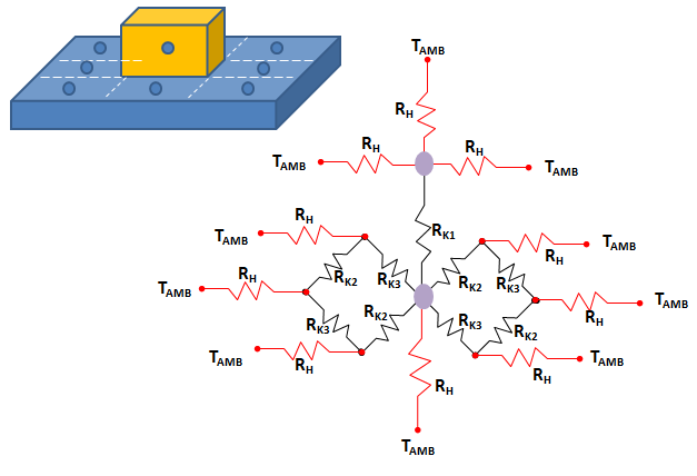
Example from application note "Basics of Thermal Resistance and Heat Dissipation" by ROHM Semiconductor.
Equivalence of Radiative Heat Transfer Rate at Low Temperature and Small Temperature Differences
Convective heat transfer rate: qCNV'' = h x [T - TREF].Radiative heat flux rate: qRAD'' = ε x σ x [TW14 - TW24] = ε x σ x [TW1 - TW2] x [TW1 + TW2] x [TW12 + TW22]
Comparing the two equations: hRAD ≡ ε x σ x [TW1 + TW2] x [TW12 + TW22]
For ε = 1.0, TW1 = 100 [°C] and TW2 = 40 [°C], hRAD = 9.23 [W/m2.K]For ε = 1.0, TW1 = 80 [°C] and TW2 = 40 [°C], hRAD = 8.41 [W/m2.K]
For ε = 1.0, TW1 = 60 [°C] and TW2 = 50 [°C], hRAD = 8.01 [W/m2.K]
As evident, the convective heat transfer coefficient in natural convection with air ranges between 5 to 15 [W/m2.K]. Hence, the contribution of radiation in natural convection cases (such as electronic cooling) is approximately equal to the convective heat transfer rate. In other words, convection and radiation contribute almost equal in natural convection heat transfer cases dealing with low temperature differences.
In general, the heat dissipation through the bodies of devices become difficult when the volume density of heat generation rate exceeds 108 [W/m3]. Such devices are often connected to the PCB with thermal vias having thickness / diameters 0.3 ~ 0.5 [mm].
Does the enclosure lead to increase in temperature of PCBA as compared to PCBA directly in contact with open surroundings? The answer is "not always"! If the enclosure is maintained as certain temperature or contains other mechanism of heat transfer (such as cold plate) - the overall air temperature in the enclosure will be lower than that in open atmosphere at fixed air temperature. Sometimes, solid walls of even lower thermal conductivities (such as 0.2 W/m-K for plastics) near hot-spots of a PCBA act as effective heat spreader.
Types of Simulations
- PCB or Package Level: Detail modelling of copper traces, thermal vias and dielectric material inside the PCB panel.
- Board Level: PCB modelled as simplified orthotropic thermal conductivity.
- Chassis Level: Similar to board-level simulation, bigger in computational domain.
- Rack Level such as in Data Centres: Most of the heat sources are modelled as lumped blocks.
Assumptions in Thermal Simulation of Electronic Assemblies
- The heat generation in copper traces must be calculated separately and data should be available to be imported in ANSYS FLUENT
- All the gaps ≤ 0.5 [mm] between solid bodies shall be filled unless they are generating heat
- All the thermal vias on the PCB board cannot be modeled (it makes the number of cells unreasonably high) - only those beneath the high heat density parts shall be modeled.
Excerpt from "HEAT AND MASS TRANSFER by Cengel and Ghajar": The failure rate of an electronic component increases almost exponentially with operating temperature. The cooler the electronic device operates, the more reliable it is. A rule of thumb is that the semiconductor failure rate is halved for each 10 °C reduction in junction operating temperature. The desire to lower the operating temperature without having to resort to forced convection has motivated researchers to investigate enhancement techniques for natural convection. Sparrow and Prakash* have demonstrated that, under certain conditions, the use of discrete plates in lieu of continuous plates of the same surface area increases heat transfer considerably.
* Enhancement of Natural Convection Heat Transfer by a Staggered Array of Vertical Plates: Journal of Heat Transfer 102 (1980), pp. 215–220.Four ways PCB are modelled in ICEPAK
"PCB is developed to mechanically support and electrically connect electronic components through conductive tracks and pads. Components are typically soldered onto the PCB to be mechanically and electrically connected to it. Many active (for example, operational amplifiers and batteries) and passive components (such as inductors, resistors, and capacitors) are mounted on the PCBs."- Hollow PCB: useful only in concept stage
- Compact PCB: all layers lumped in a single isotropic material (orthotropic thermal conductivities in all 3 directions)
- Detailed PCB: Each layer of PCB modelled with 'UNIFORM' thermal conductivity of that layer, calculated as volume weighted average of copper and substrate (FR4)
- ECAD PCB: ECAD files with detail traces and vias.
- Actual geometry of the traces and vias are not meshed along with the rest of the CFD model
- Each of the metal and dielectric layer is modelled separately
- Effect of the traces and vias is modelled in each of the CFD mesh cell by computing orthotropic thermal conductivity for the imported traces and vias.
Inputs Required for Thermal Simulations:
The inputs from PCB Design (Hardware Team) to the thermal simulation team should be provided in the format described below. The reference designators should match with the part names defined in MCAD model tree. Refer to this section to know about reference designator naming convention. Include all the parts mounted on the PCBA (whether they generate heat or not) - this is required to match the count of parts in CAD, Mesh and Report. CAD geometry: 3D model of PCBA in STEP format and ODB++ files (alternatively EMN/EMP files) are required.
In addition to heat generation rate table required as per format below, inputs required for thermal simulations are (a) Direction of mounting - to apply direction of gravity or buoyancy, (b) Empty air space around the product - if not HTC value of 5 [W/m2-K] may be used, (c) Ambient temperature for continuous operation, (d) Ambient pressure - default is sea level or 1.01 [bar] - higher altitudes reduce pressure and hence density and subsequently affects convective heat transfer rate (e) Copper layer details: each layer thickness and % copper coverage - default orthotropic thermal conductivities that can be used are 0.40, 40, 40 [W/m-K], (f) Thickness and thermal conductivity of thermal interface materials (TIM), (g) Searchable PDF file of the component placement on PCB (most of the time the reference designator names do not get imported into pre-processor).
| S. No. | Description | Ref. Designator | Qty | Vendor Part No. | Output Power [W] | Efficiency [%] | Heat Gen. Rate [W] | RθJC [K/W] | TALLOWED [°C] | Mounting type on PCB |
| 01 | ECU | E1 | 1 | LTM123 | 5.0 | 75% | 1.25 | 10.5 | 125 | Vias and pin with airgap |
| 02 | IND | L2 | 5 | MJ1201 | 0.2 | 80% | 0.04 | 2.50 | 105 | Full Contact |
| 03 | CAP | C3 | ... | ... | ... | ... | ... | 12.5 | 125 | TIM |
| 04 | IC1 | U8 | ... | ... | ... | ... | ... | Soldered pins with air gap | ||
| ... | Power Budget of the PCB Board: Energy balance helps in checking for correctness of the inputs - "worst-case estimates" sometimes have too much margin (extra heat generation rate) that may not keep the temperatures within permissible limits. | |||||||||
| ... | Total input power to the PCB Board [W]: | 20.0 | ||||||||
| ... | Total output power from the PCB Board [W]: | 16.0 | ||||||||
| ... | Heat generation in the copper traces inside PCB Board [W]: | 0.50 | ||||||||
Energy input is not same as power dissipation: Voltage regulators take power from the overall energy and make it into usable energy for circuit blocks. E.g. CPU cores are driven off low-voltage may be 1.2 [V] or lower. The IOs on CPU may be driven from a 3.3 [V] regulator. Other circuit blocks on PCB may need 5 [V], and remaining something else. Power budget needs to be arrived by supply current and supply voltage or output current and output voltage for each device on the PCB.
For linear regulators, total current is sum of all currents, regardless of voltage. For switchers, efficiency is required to calculate required current at given voltage. Power distribution network (PDN) ensures stable power supply to all electronic components. PDN consists of traces, vias, planes, voltage regulators, and decoupling capacitors. PDN distributes power from the primary source throughout the PCB board to ensure voltage supply to various components. A good source to understand basics of PCB design is "tessolve.com/blogs/power-distribution-network-in-pcb-design-ensuring-stable-power-delivery".
"Cadence's Celsius Thermal Solver and Celsius PowerDC integrate into PDN design workflows and enable PDN simulation by providing simultaneous electrical and thermal co-simulation. Celsius enables designers to visualize IR drop and Joule heating concurrently, ensuring accurate identification of thermal hotspots caused by voltage drops. Its scalable simulation capabilities allow quick iterations while maintaining accuracy, helping engineers refine decoupling capacitor placement, copper thickness, and plane structures to achieve optimal thermal and electrical performance. Additionally, Celsius supports transient thermal analysis and full 3D system-level simulations, enabling engineers to evaluate thermal dissipation strategies and airflow impacts on PDN performance, ensuring reliability and thermal efficiency in high-density designs." Reference: ema-eda.com/ema-resources/blog/pdn-simulation-optimization-emd.Heat Generation and Heat Transfer Path
The units of power and heat, both are [W] and it creates confusion while interpreting the information among power-electronics or hardware designers and mechanical thermal engineers. The heat generation rate of a device is difference between power input and power output and it is important to note that power delivered by a device to a load is not power dissipated in the device as heat. When no specific efficiency curves are available in a data sheet for the application, an assumption of the efficiency is to be considered to calculate the input power. Typically, this value can range between 70% to 90%. in case CDR (Direct Current Resistance) is known from the data sheet, it is easy to calculate heat generation rate in the device. For many devices, the power dissipation consists of two basic components - the unloaded power dissipation inherent to the device and the load power dissipation which is a function of the device loading. For example, the loading of a logic device can significantly effect the power dissipation. Most of the logic loads are capacitive, leading to more of dynamic power dissipation.The effect of radiation heat transfer is very important in natural convection, as it can contribute to approximately 25% of the total heat dissipation. Unless the components are facing hotter surface nearby such as enclosure, the radiative heat transfer must be accounted for.
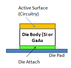
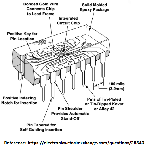
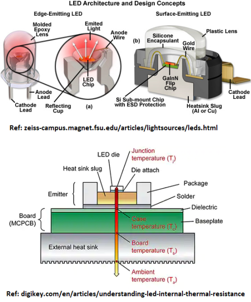
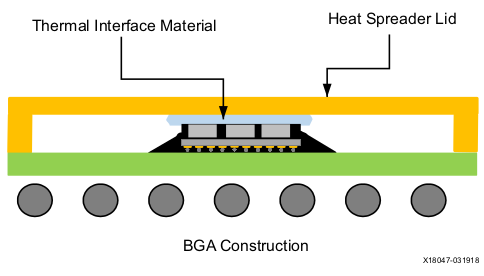
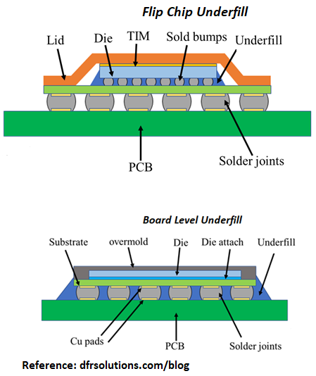
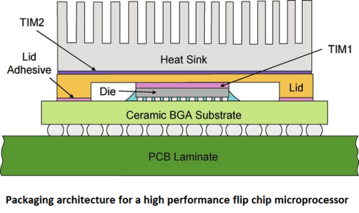
Construction Features on IC Packages
Die: It designates the piece of semiconductor on which all the active circuits lie. Dies are made of Silicon (110 – 150 W/m.K) or Gallium Arsenide (GaAs, 45 – 60 W/m.K) is used in special applications such as microwaves. The circuitry is present within a thin layer on one side only, known as active surface. The concept of "junction temperature" applies to the top surface of the die. The heat flux in the die and die-attach is very high, the junction temperature is very sensitive to the thermal conductivity and the thickness of the die and die-attach.
The Die is often attached to the substrate or the die pad by an adhesive known as the "die attach" which is made of an epoxy based compound having thickness 0.025 - 0.050 [mm] and thermal conductivity in the range 1 - 2 [W/m.K]. The semiconductor material of a die has a conductivity approaching that of a metal. If the active layer is assumed to generate constant power per unit area (an assumption that may not always be valid), the die will be practically isothermal. In practice, applications exist for which the heat flux varies significantly across the die, in which case a temperature gradient may exist on its active surface. For most packages, the thermal resistance offered by the die is small in comparison with that offered by the rest of the package. Reference: FloTHERM Pack User's Guide
Due to low thickness of the "die attach", it causes very little heat spreading. At the same time, it offers significant thermal resistance in out-of-plane direction due to its poor thermal conductivity value. Si is very widely used because of its cheap price, easiness in processing and fairly high thermal conductivity. SiC is an alternative material [though very costly] that has high thermal conductivity of 370 [W/m-K].
Die Pad or Die Flag: The Die is placed in insulated boxed often plastic packages, on a thin metal plate (made of copper and larger than the die) known as the die flag or die pad. It helps both in the manufacturing and thermal (heat dissipation) function. The metallic die flag acts as an effective heat spreader due to very high thermal conductivity of copper which can reduce the thermal resistance of a package by up to 15%.
Bond wires, made of Gold or Aluminium having diameter of the order of 0.025 [mm], are characteristics of wire-bonded packages. The number of bond wires in an IC package are of same order as the number of external leads/pins. Excerpts from "FloTHERM Pack User's Guide": In most ceramic packages, a negligible portion of the heat from the Die flows to the substrate through the bond wires. However, in plastic packages this may not be the case. Bond wires play a significant role in the heat transfer within peripheral leaded packages such as the PQFP. In area-array plastic packages such as the PBGA, bond wires can be important, especially for a 2-layer substrate.
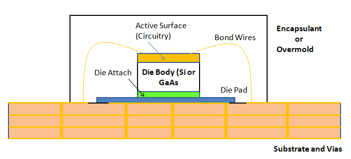
Encapsulant: Also known as 'Overmold', it is an epoxy based compound with a thermal conductivity 0.6 - 0.7 [W/m.K].
Reference: FloTHERM PACK User Guide
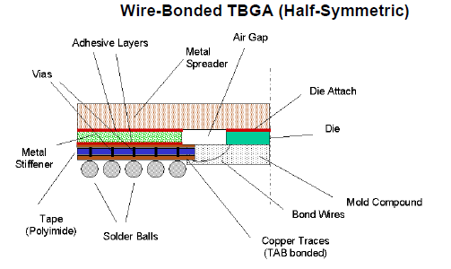
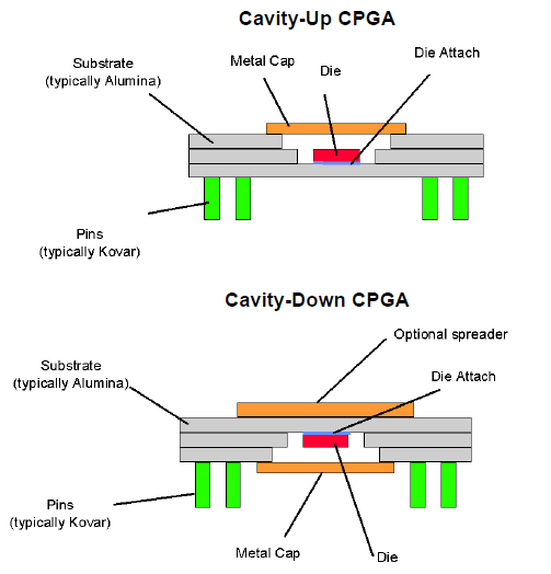
CBGA = Ceramic Ball Grid Array, PBGA = Plastic Ball Grid Array, TBGA: Tape Ball Grid Array, CPGA: Ceramic Pin Grid Array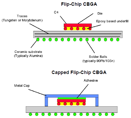
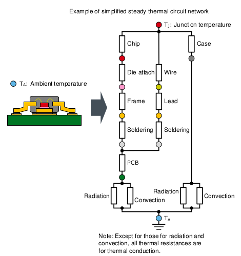
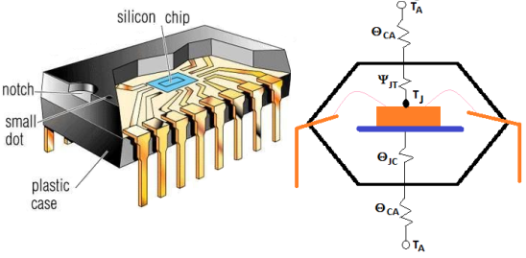
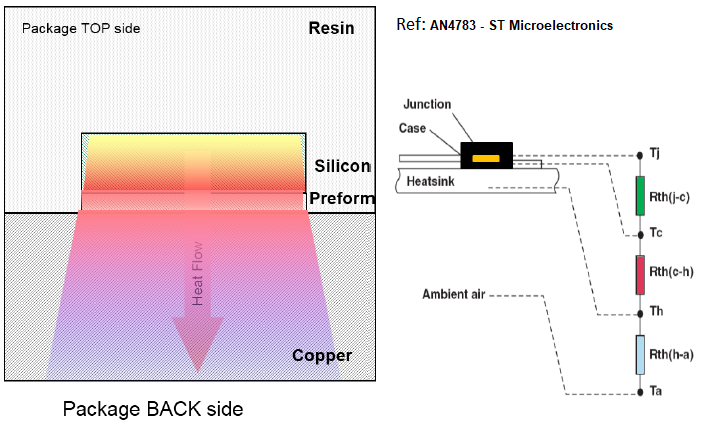
THERMAL CHARACTERIZATION OF IC PACKAGES
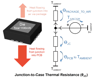
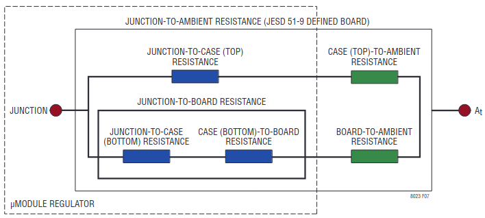
The construction of an IC (Integrated Circuit) chip is not homogeneous in 3D space. The actual heat generating segment is made-up of silicon (with thermal conductivity of 96 [W/m-K]) which will be surrounded by an Encapusulant before being attached to a Printed Circuit Board. Hence, a thermal resistance of an IC package is specified by its manufacturers which is the measure of ability of the IC package to transfer heat generated by the IC (die) to the printed circuit board or the ambient.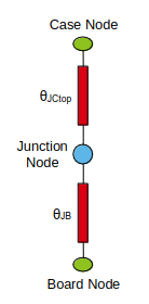
- The junction temperature is represented with a single temperature node.
- The thermal flow path is represented by a thermal resistance network.
- Junction Node represents the thermal source of the chip.
- Case Node represents the upper surface of the package.
- Board Node represents the circuit board temperature at a position of 1 [mm] from the edge of the device.
- Two thermal resistors are connected between "the junction and the case" and between "the junction and the board".
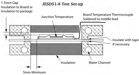
Two-resistor model is a relatively simple model achieved by dividing a package vertically at the junction and is good for single function devices. However, this model has the least precise as compared to multi-resistor network and detailed thermal models. This model (like any thermal resistor model) does not support "Transient Analyses". The methods of thermal resistance measurement are described for θJB in JEDEC Standard JESD51-8 and for θJC in JESD51-14.
In general, thermal resistance Θ or RTH = ΔT / P where P is power dissipation from the chip package in [W] and ΔT = TJ - TA.
Sample from datasheet of a DD-DC Step-down Power Supply from Linear Technology:
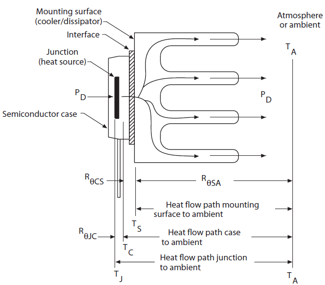
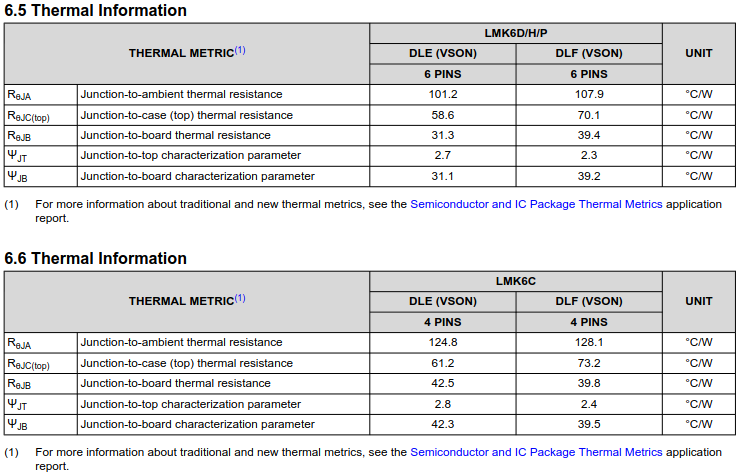
- ΘJA: also designated as RΘJA, it is the thermal resistance from Junction to Ambient, measured as [K/W]. Ambient is a generic term to thermal 'ground'. This value depends on the package design, PCB, and heat transfer modes (airflow, radiation). As per "Semiconductor and IC Package Thermal Metrics" by Texas Instruments, it is a measure of the thermal performance of an IC package mounted on a specific test coupon.
The standard test conditions are specified by Joint Electron Device Engineering Council (JEDEC) such as JESD15-3: Two-Resistor Compact Thermal Model Guideline, JESD51: Methodology for the Thermal Measurement of Component Packages (Single Semiconductor Device), JESD51-9 "Test Boards for Area Array Surface Mount Package Thermal Measurements" and JESD51-12: Guidelines for Reporting and Using Package Thermal Information.
As described in webinar "Understanding Datasheet Thermal Parameters and IC Junction Temperatures" by Monolithic Power Systems - ΘJA is valid only for its defined PCB and it is not a constant which can be used on all PCBs. ΘJA allows comparison of different packages on a common PCB.
As per datasheet for LTM8023: "θJA is the natural convection junction-to-ambient air thermal resistance measured in a one cubic foot sealed enclosure. This environment is sometimes referred to as still air although natural convection causes the air to move. This value is determined with the part mounted to a JESD 51-9 defined test board, which does not reflect an actual application or viable operating condition."Another use of RJA or ΘJA, is to calculate parameter called derating factor when the power dissipation values are unspecified in the datasheet. Using the formula TJ = TA + P × ΘJA, the permissible heat generation rate can be estimate for various ambient temperatures say between 25 [°C] to 75 [°C].
- ΘJC: also designated as RΘJC, it is the thermal resistance from Junction to Case where case is a specified point on the outside surface of the package. It depends on the thermal conductivity of package materials (the lead frame, mould compound, die attach adhesive) and on the specific package design (thickness of the die body and die attach, exposed pads and internal thermal vias). ΘJC considers only the resistance of heat flow paths to the surface of the package and hence represents only the conductive heat transfer path thermal resistance. EIA/JESD51-1 defines RΘJC as "the thermal resistance from the operating portion of a semiconductor device to outside surface of the package (case) closest to the chip mounting area when that same surface is properly heat sunk so as to minimize temperature variation across that surface".
As described in datasheet for LTM8023: "θJCbottom is the junction-to-board thermal resistance with all of the component power dissipation flowing through the bottom of the package. In the typical μModule regulator, the bulk of the heat flows out the bottom of the package, but there is always heat flow out into the ambient environment. As a result, this thermal resistance value may be useful for comparing packages but the test conditions don’t generally match the user’s application. θJCtop is determined with nearly all of the component power dissipation flowing through the top of the package. As the electrical connections of the typical μModule regulator are on the bottom of the package, it is rare for an application to operate such that most of the heat flows from the junction to the top of the part. As in the case of θJCbottom, this value may be useful for comparing packages but the test conditions don’t generally match the user’s application."
- ΘCA: it is the thermal resistance from Case to Ambient. Thus: ΘJA = ΘJC + ΘCA
- ΨJB: junction-to-board thermal-characterization parameter and ΨJT: junction-to-top thermal-characterization parameters are the "characterization parameters" that measure temperature change between the junction temperature and the temperatures of the board and top of the package respectively. These are not thermal resistances in true sense though they are useful to estimate the junction temperature when the temperature on top of the package or the board and the power dissipation are known.
As described in datasheet for LTM8023: "θJB is the junction-to-board thermal resistance where almost all of the heat flows through the bottom of the μModule regulator and into the board, and is really the sum of the θJCbottom and the thermal resistance of the bottom of the part through the solder joints and through a portion of the board. The board temperature is measured a specified distance from the package, using a two sided, two layer board. This board is described in JESD 51-9."
The Thermal Resistance is calculated in a condition where nearly all of the component power dissipation flows through either the top or the bottom of the package. In calculating the Thermal Characterization Parameter, power is the total power dissipation in the chip which can flow out of the chip through any thermal path, not just from the top or the bottom of the package.
Example Calculation - 1: A transistor with power rating of 10 [W] and internal thermal resistance of 1.5 [K/W] has a case temperature of 60 [°C]. What is the actual value of junction temperature?
Here:- Junction-to-case resistance: ΘJC = 1.5 [K/W]
- Heat generation rate ≡ Power dissipation rate: P = 10 [W]
- Case temperature: TC = TJ - P × ΘJC. Thus: TJ = 60 [°C] + 10 [W] × 1.5 [K/W] = 75 [°C]
Example Calculation - 2: A chip with 5 [W] rating has a maximum junction temperature of 120 [°C] and an internal resistance of 0.5 [K/W] at an ambient of 40 [°C] with aluminium oxide wafers. What is the maximum permissible thermal resistance of the heat sink?
- Junction-to-case resistance: ΘJC = 2.5 [K/W]
- Heat generation rate ≡ Power dissipation rate: P = 5 [W]
- Junction temperature: TJ = 120 [°C] As a "margin of safety", the permissible limit of junction temperature should be reduced by 20-30 [°C] from the value specified by the manufacturers.
- Ambient temperature: TA = 40 [°C]. In case of natural convection (passive cooling) arrangement, due to the rise in temperature caused by heating of air between adjacent fins of the heat sink, the effective value of TA should be increased by a margin of 10-20 [°C].
- Junction temperature: TJ = TA + P × [ΘHS + ΘJC]. Thus: 120 [°C] = 40 [°C] + 5 [W] × (ΘHS + 0.5 [K/W]). Hence, ΘHS = 15.5 [K/W]
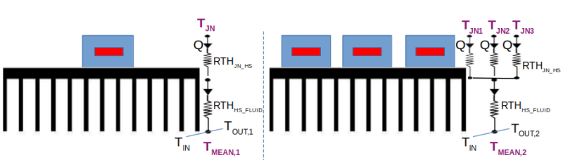
Multiple Heat Sources in Parallel on a Heat Sink
Note that the above calculation method does not apply when multiple chips are connected to same heat sink. This is because there are multiple conduction paths from junction to base of heat sink but the thermal resistance from "base of heat sink" to ambient does not change.
Excerpts from "Semiconductor and IC Package Thermal Metrics" by Texas Instruments: RΘJA is a variable function of not just the package, but of many other system level characteristics such as the design and layout of the PCB on which the part is mounted. In effect, the test board is a heat sink that is soldered to the leads of the device. Changing the design or configuration of the test board changes the efficiency of the heat sink and therefore the measured RθJA. In fact, in still-air JEDEC-defined RΘJA measurements, almost 70 ~ 95% of the power generated by the chip is dissipated from the test board, not from the surfaces of the package. Because a system board rarely approximates the test coupon used to determine RΘJA, application of ΘJA using
[TJ = TA + RΘJA × P]
results in extremely erroneous values.The document further elaborates: "In light of the fact that RΘJA is not a characteristic of the package by itself but of the package, PCB and other environmental factors, it is best used as a comparison of package thermal performance between different companies. For example, if TI reports an RΘJA of 40 [°C/W] or 40 [K/W] for a package compared to a competitor's value of 45 [K/W], the TI part will likely run 10% cooler in an application than the competitor's part." As a "margin of safety", the permissible limit of junction temperature should be reduced by 20-30 [°C] from the value specified by the manufacturers.
Excerpts from "Thermal Design Basics" by Analog Devices: In ICs, one temperature reference point is always the device junction, taken to mean the hottest spot inside the chip operating within a given package. The other relevant reference point will be either TC - the case of the device, or TA - that of the surrounding air. This then leads in turn to the above mentioned individual thermal resistances ΘJC and ΘJA. Taking the most simple case first, ΘJA is the thermal resistance of a given device measured between its junction and the ambient air. This thermal resistance is most often used with small, relatively low power ICs such as op-amps, which often dissipate 1 [W] or less. Generally, ΘJA figures typical of op-amps and other small devices are on the order of 90-100 [°C/W] for a plastic 8-pin DIP package, as well as the better SOIC packages.
Excerpts from a datasheet: "The LTM8023MP is guaranteed to meet specifications over the full –55 °C to 125 °C temperature range. Note that the maximum internal temperature is determined by specific operating conditions in conjunction with board layout, the rated package thermal resistance and other environmental factors."
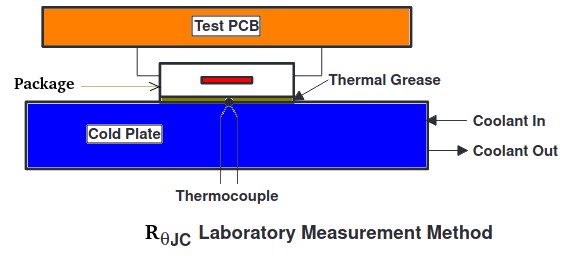
| S. No. | Field Parameter | JESD51 | Application / Thermal Simulation | Remark |
| 01 | PCB | 1.6 [mm] thick, 4.0 x 4.5[in], 2-4 layers | 6-15 layers, high thermal conductivity | 1s0p, 2s2p (s: signal layer, p: power layer) |
| 02 | Enclosure | 30 x 30 x 30 [cc] | Smaller or bigger | Enclosure shape and size irregular |
| 03 | Board position | Horizontal | Can be horizontal, vertical or inclined | Minimize convection to air |
| 04 | Package mounting | Up | Up, Down, Back-to-back | Package can be mounted on both sides of PCB |
| 05 | Measurement point | Centre of top case | Maximum in component volume | Maximum in volume is taken to make a safer estimate |
| 06 | Heat dissipation | Top face of package case only | Top face, side faces and through pins to PCB: volumetric heat source | Refer the image below for test set-up |
| 07 | Calculation of RθJC | (TJ - TC) / P | TJ = TC + RθJC x PCASE where PCASE = heat transfer through case only | RθJC remains constant |
| 08 | Recommended method | RθJC is for 'theoretical' comparison of two designs | Use ΨJT which is better representation of real world: TJ = TC + ΨJT x P | RθJC measurement 'forces' all heat to casing |
FPGA: Field Programmable Gate Array
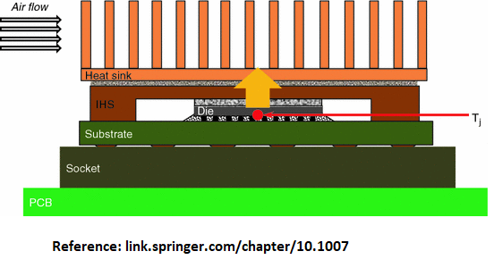
As per Intel documents for Agilex 7 FPGA: "Thermal parameters do not include the traditional junction-to-case thermal resistance (θJC) and junction-to-board thermal resistance (θJB) values, due to its multi-chip package construction." The system-level thermal analysis of this product requires the use of its compact thermal model (CTM) in a computational fluid dynamic (CFD) tool. The CTMs are simplified mechanical models of the packages with modified thermal properties so they can predict an accurate case temperature with uniform power distribution for each die. The results of the CFD analysis are valid only to evaluate the TCASE which is temperature at the top center of the IHS - (Integrated Heat Spreader, case of an FPGA) of the package. TDP: Thermal Design Power, the power dissipated in a die that is used for thermal analysis purposes.Virtex UltraScale and Virtex UltraScale+ are, ASIC-class architecture, FPGA product family from AMD. Excerpts from UltraScale+ Device Packaging and Pinouts Product Specification User Guide (UG575): "Unlike features in an ASIC or a microprocessor, the combination of FPGA features used in a user application is not known to the component supplier. Therefore, it remains a challenge for AMD to predict the power requirements of a given FPGA when it leaves the factory. Accurate estimates are obtained when the board design takes shape. For this purpose, AMD offers and supports a suite of integrated device power analysis tools to help users quickly and accurately estimate their design power requirements." The document further contains thermal resistance data with following notes: "The data includes junction-to-ambient in still air, junction-to-case, and junction-to-board data based on standard JEDEC four-layer measurements. The data in Table 10-1 is for device/package comparison purposes only. Attempts to recreate this data are only valid using the transient 2-phase measurement techniques outlined in JESD51-14. This data is not to be used in place of thermal simulation. Instead, refer to the thermal models provided for each device." In the chapter "Thermal Management Strategy", the document elaborates: "These resistances are measured using a prescribed JEDEC standard that might not necessarily reflect your actual board conditions and environment. The quoted θJA and θJC numbers are environmentally dependent, and JEDEC has traditionally recommended that these be used with that awareness."
Thermal interface material is needed because even the largest heat sink and fan cannot effectively cool an UltraScale or UltraScale+ device unless there is good physical contact between the base of the heat sink and the top of the UltraScale or UltraScale+ device. The surfaces of both the heat sink and the UltraScale or UltraScale+ device silicon are not absolutely smooth. This surface roughness is observed when examined at a microscopic level. Because surface roughness reduces the effective contact area, attaching a heat sink without a thermal interface material is not sufficient due to inadequate surface contact.
AMD advises against direct use of the θJC parameters to determine the thermal performance of the device in your application. The calculation of these parameters are done in accordance with the JEDEC standard JESD51 where system parameters differ greatly from most applications. Instead, run thermal simulations of the system in worst-case environmental conditions using Delphi thermal models, which more accurately represent the device thermal performance under all boundary conditions.
The thermal validation of FPGA thus needs to be performed using Compact Thermal Models (CTM) such as DELPHI model shown below (reference: Delphi Compact Thermal Model Guideline).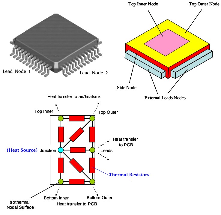
Efficiency and Power Losses in MOSFETS
Reference: MOSFET power losses and how they affect power-supply efficiency - by By George Lakkas, Product Marketing Manager, Power Management
MOSFETs have a finite switching time, therefore switching losses come from the dynamic voltages and currents the MOSFETs must handle during the time it takes to turn on or off. MOSFET switching losses are a function of load current and the switching frequency of power supply. There are 3 types of losses: conduction losses, switching losses and static (quiescent) losses.
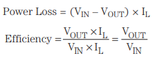
Most of the power is in the MOSFET gate driver. Gatedrive losses are frequency dependent and are also a function of the gate capacitance of the MOSFETs. When turning the MOSFET on and off, the higher the switching frequency, the higher the gate-drive losses. This is another reason why efficiency goes down as the switching frequency goes up.
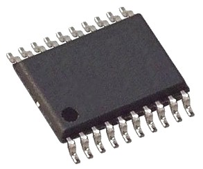
MOSFET
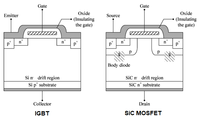
Discrete power devices are the workhorses for power management and conversion of the most systems which fuel the central processing units and digital signal process ICs. Typical discrete products include various Diodes, Bipolars, metal-oxide-semiconductor field effect transistors (MOSFET) and Insulated Gate Bipolar Transistor (IGBT)s. A MOSFET may look like a black box from outside as shown below. However, inside the insulating enclosure contains many heat dissipating components consisting of silicon, copper and soldier joints. Capacitors and metal-oxide-silicon field effect transistors (MOSFETs) are the main elements in the ECU, which generate heat during operation, due to the Joule effect. In addition, capacitors and MOSFETs also generate heat due to electro-chemical reactions, dielectric losses and entropy changes. "The insulated-gate bipolar transistor (IGBT) was developed to overcome the drawbacks of bipolar transistor of low current gain, by combination of MOSFET and bipolar transistor."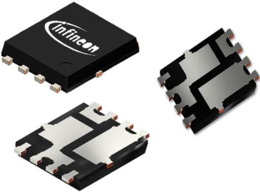
Construction of an IGBT referenced from Fuji Electrical application notes and Toshiba Semiconductor website.
An IGBT is a device with a MOSFET structure for input and a Bipolar Junction Transistor (BJT) structure for the output. Thus, it exploits the benefit of MOSFET (having higher input impedance and fast switching speed) and BJT (having low on-voltage even when subject to high voltage).
Cross-section view as per article "Critical solder joint in insulated gate bipolar transistors (IGBT) power module for improved mechanical reliability" by Nebo et. al. are shown below.
The smallest working unit of an IGBT package consists of two chips: IGBT chip and Free-Wheeling Diode (FWD) chip. FWD chip allows current to flow smoothly when the IGBT is turned off (while switching). SiC SBD (Schottky Barrier Diode) chips or traditional Si FRD (fast recovery diode) are used as FWD. An IGBT module may put multiple IGBT/FWD chips together within same encapsulation enabling higher power handling capacity and stronger construction. Ceramic substrate layer in Direct Bond Copper board (DBC: copper layers metallurgically bonded directly to both sides without any adhesive) provides electrical insulation while allowing heat to transfer from chips towards heat sink. Solder in the joints is typically lead-free alloy of 96.5% tin, 3% silver, and 0.5% copper (SAC305) composition.
Typical thickness values are: Chip [0.1 mm], solder [0.1 mm], DBC top copper [0.3 mm], DBC ceramic [0.4 mm], DBC bottom copper [0.3 mm], DBC solder [0.08 mm], Base plate copper [1.5 mm]
Typical material properties are: Chip [2300 kg/m3, 140 W/m-K, 700 J/kg-K], Solder [7400 kg/m3, 50 W/m-K, 230 J/kg-K], Ceramic [3900 kg/m3, 20 W/m-K, 900 J/kg-K]
Notice the empty space inside the resin cover is filled with potting material. CoolTherm SC-324 from Parker is a two-component mixture silicone encapsulant which provides excellent thermal conductivity while retaining desirable properties associated with silicones. The material specification as published on the supplier website is:- Dynamic Viscosity at 25°C:
- Resin: 37,000 cP
- Hardener: 43,000 cP
- Mixed: 30,000 cP
- Cure Time: 24 Hours at 25°C and 60 min at 125°C
- Thermal Conductivity: 4 W/m-K
- Dielectric Strength: 7.4 kV/mm


Reference: AN90003 - LFPAK MOSFET thermal design guide
- Part number BUK7M15-60E (LFPAK33, 15 mΩ, 60 V) the maximum thermal resistance junction to mounting base is 2.43 [K/W], the total thermal resistance, junction-to-ambient is 59.4 [K/W] when using 65.4 °C as (ambient) reference point.
- Part number BUK7S1R0-40H (LFPAK88, 1 mΩ, 40 V) the maximum thermal resistance junction to mounting base is 0.4 [K/W], the thermal resistance between mounting base and ambient is of much higher value (~ 30 K/W)
The list of Joint Electron Device Engineering Council (JEDEC) standards related to thermal characterization of IC chips are:
- JESD51: Methodology for the Thermal Measurement of Component Packages (Single Semiconductor Device)
- JESD51-1: Integrated Circuit Thermal Measurement Method—Electrical Test Method (Single Semiconductor Device)
- JESD51-2: Integrated Circuit Thermal Test Method Environmental Conditions—Natural Convection (Still Air)
- JESD51-3: Low Effective Thermal Conductivity Test Board for Leaded Surface Mount Packages
- JESD51-4: Thermal Test Chip Guideline (Wire Bond Type Chip)
- JESD51-5: Extension of Thermal Test Board Standards for Packages with Direct Thermal Attachment Mechanisms
- JESD51-6: Integrated Circuit Thermal Test Method Environmental Conditions—Forced Convection (Moving Air)
- JESD51-7: High Effective Thermal Conductivity Test Board for Leaded Surface Mount Packages
- JESD51-8: Integrated Circuit Thermal Test Method Environmental Conditions—Junction-to-Board
- JESD51-9: Test Boards for Area Array Surface Mount Package Thermal Measurements
- JESD51-10: Test Boards for Through-Hole Perimeter Leaded Package Thermal Measurements
- JEDEC51-12: Guidelines for Reporting and Using Electronic Package Thermal Information
Some other examples are:
Commercial Tools for PCB Design and thermal simulations
- ANSYS ICEPAK: A customized GUI for pre- and post-processing but uses FLUENT as solver.
- SIEMENS FloTHERM: similar in look and operation like ICEPAK with primitives, SmartPart and attributes.
- Electrical Packages such as PSPICE and Cadence (new owner of 6SigmaET): These packages primarily meant for design of IC chips has thermal modeling capabilities to check 'what-if' scenarios. Other EDA (Electronics Design and Automation and sometimes also used for Exploratory Data Analysis) tools are Allegro, Board Station, Expedition and CR5000.
- ECXML format for Thermal Simulations is equivalent to STEP format for CAD tools. The data from ICEPAK to FloTHERM can be transferred in ECXML format which is a vendor neutral format.
- DELPHI: Compact Thermal Model - the standard to create a thermal model for further use in thermal simulations
Heat Generation Rates in Electronic Parts
Capacitors: P = (2πf * C)2 · ESR · V2 where C is capacitance [F], ESR is Equivalent Series Resistance [Ω], f is frequency [Hz] and V is Voltage [V]. Other terms associated with capacitor heat generation are δ = defect angle and tan(δ) = dissipation factor: tan(δ) = ESR · 2πf · C
- Power Density, PD: The power density of any device is the ratio of output power and the physical space it occupies. Thus, the unit of power density is [W/m3] or [W/cc].
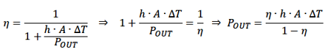
- Efficiency, η: This is the ratio of output power and the input power, η = POUT / PIN. The loss of energy (or power) gets converted into heat. Hence, when power density is increased, the volume and surface area of MOSFET and any such device will decrease. To keep temperature rise of the system within permissible limit, the amount of heat dissipation has to be decreased which in turn require that the efficiency of the device must be increased. The efficiency data is available in datasheets such as the one shown below for a DC-DC Step Down Power Supply (LTM8023):
Note that the calculated value as per method described below for heat gneration (Power Loss) does not match with the graph provided in the datasheet.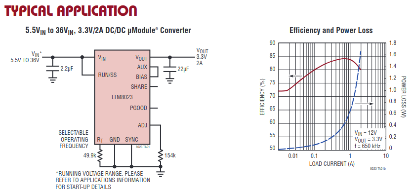
- Heat generation rate = PIN - POUT = (1 - η).POUT = (1/η - 1).PIN and the efficiency values of are available in datasheets published by the manufacturers. For example, if the output of a device is 5 [A] at 3 [V] and efficiency is 75%, the heat generated in the device would be (1.0-0.75).(3 × 5) = 3.75 [W].
- Heat dissipation: q = PIN - POUT = h x A x [TS - TAMB] where h is the convective heat transfer coefficient of the surface exposed to cooling media, A is the skin (fluid-wetted) surface area, TS is the surface temperature of the device casing and TAMB is the bulk mean temperature of cooling media.
- Efficiency: η = POUT / PIN = POUT / [POUT + q]
- η = 1 / [q/(V x PD) + 1] where V = volume of the device
- η = 1 / [h x A x ΔT/(V x PD) + 1] where ΔT = [TS - TAMB]
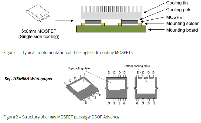
The DSOP Advance package has a top source side cooling plate in addition to the bottom drain side plate as shown in Figure 2. These cooling plates contribute in reducing the thermal resistance (Rth).
Reference: TOSHIBA Technical Application Note
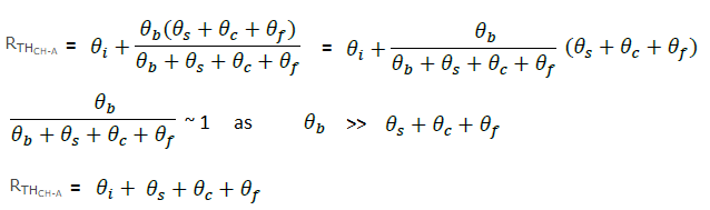
At thermal equilibrium, the maximum power dissipation PDMAX of a power MOSFET can be expressed in terms of the ambient temperature TA, the maximum channel temperature TCHMAX of the MOSFET and the channel-to-ambient thermal resistance RTHCH-A
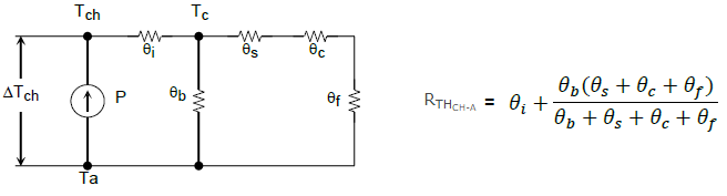
- θi: Internal thermal resistance (channel-to-package)
- θb: External thermal resistance (package-to-ambient air), varies with the material and shape of the case and is significantly larger than θi, θc, θs and θf.
- θs: Thermal resistance of insulation shield
- θc: Contact thermal resistance (at the interface with a thermal fin)
- θf: Thermal resistance of the heat sink
| Component | Material | Thermal Conductivity [W/m-K] | Density | Specific Heat Capacity [J/kg-K] |
| Capacitor | Aluminium Oxide | 30 | 3890 | 880 |
| MOSFET | Silicon | 80 ~ 150* | 2390 | 712 |
| Thermal Grease | SiC | 0.42 | 2500 | 750 |
Reference - [AN90003: LFPAK MOSFET thermal design guide] "The PCB material FR4 has a maximum operating temperature of around 130 [°C], depending on manufacturer and chemistry, this is much lower than the limit specified for the junction of a silicon die (175 °C)".
Netlists
As per resources.altium.com/p/what-are-netlists-pcb-design-projects: "All netlists are defined at the circuit level and are constructed by CAD tools from circuit diagrams in schematic sheets. A schematic editor will create netlists as you place components and draw circuits, either automatically or with a manual compiler tool. The netlist can then be used in other CAD systems, such as in a SPICE simulation program or a PCB editor. Because all netlists define electrical connections between components, they are created from circuit drawing tools or schematic capture programs. Schematic netlists used in PCB design software, whether in Altium Designer or another PCB CAD tool, are then used to define the connectivity between component pads in a PCB layout."Trace Heating in PCB
A net is a set of electrically connected traces and pins. A PCB trace is a thin sheet of conducting copper placed on a non-conductive base material usually called FR4 that carries the signal and power to the whole circuit. A copper trace has a specific width called trace width, and a particular thickness. The thickness of PCB is specified in ounce/ft2 = 28.35 gm/ft2 = 0.3052 [kg/m2] = 0.3052/8900 = 3.43 x 10⁻⁵ [m] = 0.0343 [mm]. For typical PCBs, the most common copper thickness is specified as 35 [μm] which is equivalent to 1.0 [oz/ft2]. With electrical resistivity of 1.72 x 10⁻⁸ [Ω.m] at 25 [°C] for copper, the electrical resistance per inch width per meter length of copper trace is 0.02 [Ω]. The electrical resistance per inch width per inch length of copper trace would be 0.50 [mΩ]. The resistance value shall increase in direct proportion of the length and inverse proportion of the width and/or thickness (mm or oz/ft2).
For example, electrical resistance per inch width per inch length of copper trace having thickness of 2.0 [oz/ft2] would be 0.50 / 2 = 0.25 [mΩ]. Electrical resistance per 0.1 inch width per inch length of copper trace having thickness of 2.0 [oz/ft2] would be 0.50 / 2 / 0.1 = 2.5 [mΩ]. Electrical resistance per 0.1 inch width per meter length of copper trace having thickness of 1.0 [oz/ft2] would be 0.50 * 39.37 / 0.1 = 0.197 [Ω]. With temperature coefficient of electrical resistance 0.0039 [1/K], electrical resistance per 0.1 inch width per meter length of copper trace having thickness of 1.0 [oz/ft2] at 100 [°C] would be 0.197 x [1 + 0.0039 x 75] = 0.255 [Ω]
Trace Heating: In the electrical wires the cooling rate initially increase with thickness of insulation, reaches a peak and then starts decreasing. Similarly, the temperature of traces are dependent on the board thickness, traces on top of a thin board get hotter than one on a thicker board. This is because a thicker board has higher cross-section for the heat to conduct through. Beyond a thickness of board, there is more material under the trace than the trace can efficiently utilize - the path to surface on which convection occurs gets longer - and hence there is no improvement in temperature or in fact the temperature of traces may increase further. PCB trace temperatures are very sensitive to thermal conductivity though the in-plane thermal conductivity has higher influence than through-plane value.
For a detailed explanation of Joule Heating and coupling between SIwave-ICEPAK-Mechanical, refer to the article "How To: Thermal Simulation with ANSYS" from electronicsforu.com/electronics-projects/electronics-design-guides/taking-the-heat. An accurate check of voltage differences (drops) and currents for all traces (including ground planes) is must before passing the board for thermal simulations or to manufacturing. Trace heating is usually due to DC current and is calculated using DCIR simulation. The effect of AC on PCB circuit is evaluated as Power and Signal Integrity simulations. As per Altium: "Power integrity refers to the stable delivery of power to all components on a PCB. Inadequate power integrity can lead to voltage fluctuations, which in turn cause signal integrity problems like jitter, noise, and timing errors."Polygon or irregular or rectangular copper pours represent areas of copper that extend beyond traditional traces on a PCB creating large conductive areas that can be assigned to particular nets, most commonly ground or power. These are different from standard traces that connect specific components. Placing copper pour means filling unused space of a PCB layer with planar copper.
This article ansys.com/en-in/blog/thermo-mechanical-analysis-pcb describes 3 methods generally used for thermo-structural analysis. If one is interested in temperature of individual traces, there is no other option but to model the entire board explicitly by extracting the full 3D geometry of the PCB layout where each trace and via is modeled in detail.
Image showing traces and connection of pins: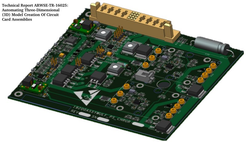
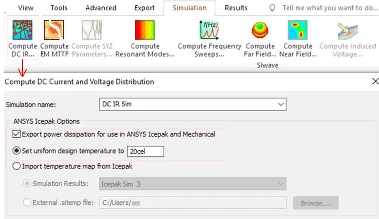
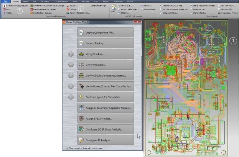
SIwave - ICEPAK Coupling
The coupled simulation between SIwave DCIR analysis and ICEPAK thermal simulation can be performed by running independent Icepak simulation (outside of the Electronics Desktop) wherein heat source in PCB layers are imported by .out/.outb powermap files obtained as a power map export after DCIR simulation in SIwave. This file contains the calculated distributed heat source data. DCIR stands for Direct Current Impedance and Resistance and sometimes Direct Current Internal Resistance. The blog post titled "DCIR Analysis of PCB using ANSYS SIwave" at leapaust.com.au/blog/emag/dcir-analysis-of-pcb-in-ansys-siwave is a good demonstration of SIwave features.- Step-1: Open ICEPAK and import the PCB geometry into Icepak using a supported format such as ODB++ as per method described here
- Step-2: Create enclosure around the PCB to represent air domain
- Step-3: To define heat sources, import the power map by selecting the *.out or *.outb file exported from SIwave
- Step-4: Define the remaining thermal boundary conditions such as ambient temperature, gravity, fan in case of forced convection...
- Step-5: Set up heat sources for components not included in the SIwave analysis
- Step-6: Generate Mesh, apply Solver Setting and make Run. Add current sinks (IC chips, RAM, FPGA... which consume power) and voltage sources (SMPS - Switching Mode Power Supply, switching regulators, buck converters, batteries, linear regulators...)
- Step-7: Post-process as needed, generate power-tree diagram, plot current density, and power loss distributions.
100 percent conductivity corresponding to a resistivity of 0.153022 ohm/meter-gram at 20 °C. The value assumed by the Bureau of Standards as representing "Matthiessen's standard", an standard in wide use commercially. This value corresponds also to 1.72128 micro-ohms/cm3 at 20 °C on an assumed density of 8.89 [g/cc]. The distortions caused by bending and winding a wire are shown to produce no material change in the temperature coefficient.
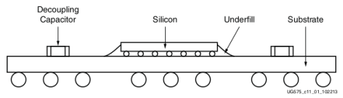
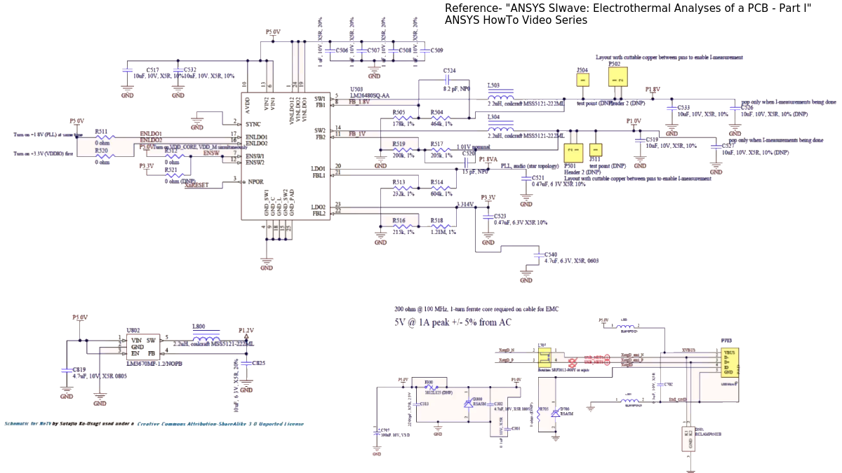
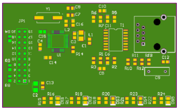
The schematic of the PCB shown above is displayed below. Note that schematics are logical and do not contain spatial information. They show how components are connected electrically and not where they are placed physically. The process of transformation of a circuit diagram into the physical layout (placing routing traces and components on a board) is called PCB Layout generation. The diagram below has 6 power nets and 2 ground nets.
Ground Planes in PCB Layers
As per article, "resources.pcb.cadence.com/ blog/ 2020-the-pcb-ground-plane-and-how-it-is-used-in-your-design", "Almost every component on the PCB will connect to a power net, and then the return voltage will come back through the ground net. On boards with only one or two layers, ground nets usually have to be routed using wider traces. By devoting an entire layer to the ground plane in a multi-layer board however, it simplifies connecting each component to the ground net." Thus, ground plane can either be a designated area of metal on a circuit board layer, or it could take up the entire layer itself.Every signal that travels through a trace on a PCB must have a return current that flows back to its source, taking the path of least impedance. As per article sierraassembly.com/blog/what-is-pcb-ground-plane: "In PCB design, a ground plane is a conductive layer built into the board architecture that acts as a common reference point for electrical signals and currents. Its primary function is to provide a low-impedance channel for returning currents while maintaining a steady ground potential throughout the circuit. Since all conductors have non-zero DC resistance, heat is generated in ground planes too as they must carry some current. The ground plane helps with thermal management by acting as a heat sink, removing excess heat from components and dispersing it across the PCB surface."
Industry standards used to calculate trace cross-sections required to keep temperature rise limited: (a) IPC-2221 - General-purpose design standard to make conservative estimates of trace resistance and (b) IPC-2152 - Accurate standard that incorporates planes into models for trace heating.As per "resources.pcb.cadence.com/blog/er-grounding-and-return-paths-power-plane-no-nos": Good power plane design involves continuous, unbroken planes that provide a stable reference for signals and a low-impedance path for current. Every signal layer should have a solid reference plane directly adjacent to it, and power planes should be carefully managed to avoid unnecessary segmentation. Stitching vias are vertical connections between ground or power planes on different layers of the PCB. Their purpose is to maintain return path continuity when signals transition between layers, especially during high-speed routing. Without them, return currents can be forced into convoluted paths that increase loop area and inject unwanted noise into the system.
Even if the return current is sum of currents in all traces and occupies only a narrow region of the ground plane (say a few mm wide under a signal trace), that region still has a huge cross-sectional area compared to thin traces. The return path widens gradually near vias, pads, and power return regions thereby adding parallel current paths. The plane is a continuous sheet and hence the current can laterally spread as needed keeping the potential gradient small, which means lower effective resistance. On the other hand, ground planes are filled with holes where tens if not hundreds of vias punch through them, which obstruct return current.Capacitance of PCB: Due to layered structure of PCB, it acts like many "parallel plate capacitors" connected in series and parallel arrangement.
IDF and IDX: ECAD - EMN/EMP
The emn file contains the dimensions of the board, the size and placement of all through holes, and the placement of all components. The emp file describes the individual components used on the board.
Some key features of such simulations are usage of Intermediate Data Format (IDF) and Incremental Data eXchange (IDX) files that have been exported from an ECAD package. These files contain informations of traces in PCB. In ANSYS ICEPAK, while importing traces the default materials are Cu-pure for metal and FR4 for dielectric.PCB construction is a layered design along the thickness direction and hence the thermal conductivity is necessarily orthotropic. Here, the conductivity value along the thickness direction - known as through-the-plane conductivity is far less than in-the-plane conductivity values. .emn file supports importing the data into a part that would represent the PCB or panel without any component placement. The .emn file has a section for the placement info with the header that can be edited in a text editor to delete it. This section starts with ".PLACEMENT" should you need to remove the placement data from the file. The IDF files are text files and can be easily manipulated by scripting tools such a Python and PERL. Section 3.10 of the IDF 3.0 specification which defines how drilled holes are handled. In summary:
- EMN File Contains:
- PCB Outline
- Component Location
- Component Orientation
- Hole Information
- Keep In and Keep Out Regions
- EMP File Contains:
- ECAD outlines for every component
- ECAD component height information
There are many programs used to generate design of electronic items such as PCB and chips. Zuken, Cadence, EasyEDA, Eagle, Altium Designer, Siemens Expedition Enterprise to name few. However, there is a need to have interface between ECAD and MCAD. This is accomplished by EMN and EMP files. The EMN file is related to the board and the EMP file is the library list of the components on the board. These files can generate a 3D view of the PCB Assembly. IDF files default to the following extensions: *.emn - neutral file of the board outline and component placement and *.emp - profile file that contains component outlines.. A sample EMN file commented with explanation of the information can be found here.
While reading .EMN file in other MCAD programs such as ANSYS Discovery, Creo, FreeCAD and SolidWorks, the model tree may contain only the names of size designators and reference designator or actual part number may be missing. A reference designators are combination of letters and numbers assigned to PCB components, such as resistors, capacitors, and other electronic elements which provide a standardized way to identify and reference components on the board.This may only give a good representation of the board but one cannot do further processing such as assigning heat generation rates, material properties...To get Mechanical Models with different part names, ECAD Design Software should be set to output package types as the ecad_name and (a) either an internal corporate part number or (b) a vendor part number as the ecad_alt_name. Do not set up ECAD IDF output to use identical ecad and ecad_alt names. AR = Amplifier, C = Capacitor, D = Diode, F = Fuse, FB = Ferrite Bead, J = Connector / Jack Connector, K = Relay, L = Inductor, LED = Light Emitting Diode, M = Motor, P = Plug, PS = Power supply, Q = Transistor, R = Resistor, S = Switch, T or XMER = Transformer, TP = Test Point, TR = Transistor or transducer, U = Integrated Circuit, Z = Zener Diode. For example, R1 might refer to the first resistor on the board, C2 could be the second capacitor, and U3 might represent the third integrated circuit. More information at resources.altium.com/p/altium-designer-helps-you-track-reference-designators-your-pcb such as the image below.
ECAD to MCAD
The changes which are required to convert ECAD data to MCAD (STEP format) include conversion of zero thickness traces / copper planes into thin solids, checking the gaps between parts and merging those with ≤ 0.2 mm gaps.The ECAD software may allow special characters such as @, #, $ and % in item names. The MCAD data should replace these characters to alpha-numeric values. Optionally but recommended: the MCAD data should group the parts into the categories of reference designators.
Some of the pre-processors for CFD simulations such as SpaceClaim and Discovery do not import each reference designator as unique body. The ECAD to MCAD conversion should ensure that each body on the PCBA has unique name explicitly define before exporting to STEP format.STAR-CCM+ 19.06 was able to read reference designators as bodies from STEP file generated by Zuken but could not read them at all from a STEP file generated by Allegro. One of the critical issue in ECAD to MCAD is the creation of model tree where items are named as either the reference designators or the item names contain reference designator strings in some form.
Reference: simplifiedsolutionsinc.com/images/Steps-to-create-3D-PCBs-in-ProE.pdf: In Pro/E (predecessor to Creo), there was an option to create an ecad_hint.map file which linked components in CAD Tool to 3D Pro/Engineer Model. When an IDF (emn) File is imported into Pro/Engineer, Pro/E cross-referenced the ecad_name and ecad_alt_name from the emn file against the ecad_hint.map. If a match was found, Pro/Engineer replaced "on the fly" geometry with a real 3D Pro/Engineer part or assembly. More information can be found at support.ptc.com/.../Map_File_Standard_Conventions.html
Sample ecad_hint.map file. Each section begins with the purpose, followed by '->'. Each section ends with 'end'. # is the comment character. Wildcard (*) is valid for 'all'. Object and value fields are separated by a space, spaces are permitted in value strings if the string is surrounded by quotation marks.
mcad_in_ignore -> or map_objects_by_name ->
ecad_name "resistor"
ecad_alt_name "res_5"
ecad_type "part"
mcad_name "m_part"
mcad_type "part"
ref_des "*"
end
As per Alitum documentation under "Mechanical Data Import-Export Support": "In the STEP file, each component is identified by its designator. If the MCAD designer needs to import multiple boards into a single MCAD file there is likely to be designator clashes, to avoid this include a Component Suffix."
Many a times, MCAD generation is aimed at mechanical integration alone and hence copper-traces are just dropped for better performance. For cases where copper traces, pins, vias and solder joints are needed for structural and thermal analyses, additional steps are required in MCAD environment.
PWA = Printed Wiring Assemblies. Excerpts from "Intermediate Data Format Specification, Version 3.0": Structure of the Intermediate Data Format - The Intermediate Data Format consists of three files: the Board File, the Library File and the Panel File.
The Board File (.emn or .bdf): It contains a description of a single PWA, including the board shape, layout restrictions and component placement.
The Library File (.emp or .ldf): It contains descriptions of components used by one or more PWAs. *.emp is the extension of the library file.
The Panel File: It contains a description of a manufacturing panel including the panel shape, layout restrictions and the placement of boards and components on the panel.
Data is organized by sections in these files. Each section begins with a keyword indicating the type of data the section contains and a matching keyword at the end of the section. They are .PLACE_KEEPOUT, .BOARD_OUTLINE, .ROUTE_OUTLINE, .DRILLED_HOLES. All data between the section keyword and its corresponding ending keyword pertains to that section. Sections cannot be nested. Unless otherwise noted, sections within a file can be in any order. Data within the sections is represented by one or more records consisting of one or more fields. Each line in a file is a separate record: fields within a record are separated by one or more blanks. Records within a section and fields within a record must be in a specific order. Records are free format which means that the fields they contain can be any length, and each field can begin in any column as long as the order of fields is maintained.
The Panel File is an optional file, similar to the Board File, that contains the physical description of a manufacturing step-and-repeat panel and the locations of boards and components on that panel. The Panel File references one or more PWAs described in separate Board Files. Any component placed on the panel itself is referenced in a Library File.
Note: "The comment character is the pound or hash sign (#). A comment must be a separate line (record) and the comment character must be in column 1. Comments should be located between, but not within sections of the IDF files." The Header section must be the first section in the file, the second section must be the Outline section, and the last section must be the Placement section. All other sections may be in any order. Exporting IDF files in Atlium wil1 generate two files - one containing information about the physical size and shape of PCB and positions of components, the other containing information about each component including name, size, and shape. These are typically referred to as the board and library files, respectively. Different CAD packages use different file extensions for the board and library files. The board file and library file extensions of generated files have following pairs: .brd and -pro, .brd and .lib, emn and emp, . bdf and.ldf, .idb and .idl, .idf and .lib. Note that EMP is for describing parts that equip the board. Thus, for a PCB (without parts on it), no EMP file will be generated.The Gerber file
It is a connector and bridge between designers, engineers and PCB manufacturers. It needs to go through every manufacturing process and the factory can clearly define the customer's needs. According to UCAMCO (the company that currently owns the rights to Gerber File format): "Gerber file format" is a standard for PCB design data storage or transfer. Gerber file describes and communicates the constituents of a PCB image like the number of copper layers, solder masks and many others such attributes. Gerber files also act as input files to PCB printing devices like photo-plotters and Automated Optical Inspection (AOI) machines to print or compare circuit board images for different gadgets. Gerber files may also include metadata (data about other constituting data within a file) like solder mask, legend/silk and number of copper layers among other relevant printing information.
Following files comprise the full list of GERBER files which are usually zipped and shared to thermal simulation engineer or PCB Manufacturer. An open-source program Gerbv to view Gerber files can be found at https://gerbv.github.io.
| Gerber File Type | Extension |
| Top side (copper) Layer | .GTL |
| Bottom side (copper) Layer | .GBL |
| Top Overlay | .GTO |
| Bottom Overlay | .GBO |
| Top Paste Mask | .GTP |
| Bottom Paste Mask | .GBP |
| Top Solder Mask | .GTS |
| Bottom Solder Mask | .GBS |
| Keep-Out Layer | .GKO |
| Drill Drawing | .GD1 |
| Drill Guide | .GG1 |
| Internal Plane Layer 1, 2 ... 16 | .GP1, .GP2 ... .GP16 |
Refefence from "Automating Three-Dimensional (3D) Model Creation Of Circuit Card Assemblies - Technical Report ARWSE-TR-16025": ECAD software suite is typically used to perform the initial step of designing the electrical circuit. A schematic is generated that depicts electrical components using different symbols and depicts their electrical interconnections using lines between 'pins' on the components => Once the schematic is complete, the software generates a 'netlist' that defines how the various components are interconnected => The netlist is imported into a separate application within the ECAD suite, which is used to design the physical printed wiring board design from the functional design created by the schematic => The board design software then exports industry standard files that describe to a manufacturer how the circuit boards are to be fabricated => Mechanical CAD (MCAD) software is used to perform three-dimensional (3D) modelling and analysis. This is the preferred tool for visually verifying the correct placement and orientation of the components on a PCB.
Reference: resources.pcb.cadence.com/blog/what-is-a-pcb-netlist - A PCB netlist is an ASCII text file that defines a circuit’s electrical connectivity by listing all connections (nets) between component pins. Unlike a schematic, which visually represents the circuit with symbols and connections, a netlist focuses solely on conveying essential connectivity data for PCB layout, simulation, and other EDA tools. Common netlist formats include EDIF (Electronic Design Interchange Format), IPC-2581, and SPICE (.CIR)
ODB++
Refer odbplusplus.com/design/our-resources for more information. A non-proprietary format ODB++ was developed in 1992 by Valor Computerized Systems Ltd now owned by Siemens. A "Sample ODB++ version 8.1 File" is available as .tgz zipped file (organized as a multilevel directory tree) which contains following folders: fonts, input, matrix, misc, output, steps, symbols, user, wheels, whltemps.
ANSYS Electronic Desktop (AEDT) can read ODB++ files in *.tgz (which is same as *.tar.gz) format only. Ensure that there is no special character such as + or $ in the file name or file path.Open DataBase (ODB)++ file format is an alternate to Gerber which conveys all the required information to a PCB manufacturer. ODB2GBR program from Artwork Conversion Software, Inc converts an ODB++ into Gerber format. "ODB++ is a manufacturing-oriented product model data format, containing all the necessary data for fabrication, assembly and test in a single file structure." From altium.com: "ODB++ is a CAD-to-CAM data exchange format used in the design and manufacture of printed circuit boards."
The following files and directories are mandatory where words in italics are user-specified.- product_identifier/matrix/matrix: represent the basic layer characteristics: name, type, subtype, context, polarity, reference, and dielectric reference.
- product_identifier/misc/info
- product_identifier/fonts/standard
- product_identifier/steps/step_name/stephdr
- product_identifier/steps/step_name/layers/layer_name/features - Product model layers can contain graphics, properties and annotation. Layers express physical board layers, and also mask layers, NC drill and rout layers, and miscellaneous drawings.
From format specifications: "Steps are multi-layer entities such as a single image, an assembly panel, a fabrication panel, or a fabrication coupon. Each step contains a collection of layers. Layers are two-dimensional sheets, containing graphics, attributes and annotation. Layers express physical board layers, mask layers, NC drill and rout layers and miscellaneous drawings. All steps in one product model have the same list of layers, even though the contents might be different."
From format specification: "There are links between files, defined implicitly in the ODB++ definition, that create dependencies between files. For example, the file /step_name/layers/comp_+_top/components contains links to /step_name/ eda/ data, and the /step_name/ layers/ layer_name/ features file contains links to user-defined symbols located in product_model_name/symbols."
Units: The default units of measurement for the product model are as defined in the UNITS directive in the file misc/info of the product model. If the default is not defined for the product model, the default is imperial.
PCB Outline:
The outline is usually found within the 'features' file of a specific 'mechanical' layer (layers/mechanical*/features). /step_name/layers/profile/: The profile layer is used by fabricators for board routing (cutting the board out of the panel) and for DFM (Design for Manufacturability) checks to ensure no components are placed outside the board boundaries. profile/features contains geometry commands such as: L: Line Records, A: Arc Records, P: Pad Records, T: Text Records, B: Barcode Records and S: Surface Records. The parameter 'I' or 'M' can be added at the end of the line to indicate that the dimensions in this symbol name are expressed in imperial units or metric units.The file consists of the UNITS, ID, and F records (number of features), a section that lists symbol names, an attribute lookup table, and lines or structures defining the various types of features. Each line, pad, or arc feature definition record lists the index of the symbol used to construct that feature.
Format of the line is: ormat of the line: $serial_num symbol_name [I|M]. Example of symbols (geometric primitives) are: $0 r5: 5 is circle diameter, $1 s10: 10 is square side, rect12x15: 12 is width and 15 is height of the rectangle, oval: rectangle with full round on width dimension. hole5xpx0.01x0.05 where 5 — Hole diameter, p — Plating status plated, non-plated or via, 0.01 — Positive tolerance, 0.05 — Negative tolerance - Intended for wheels created for drill files. There are 45 different shapes available.Line example: L xs ys xe ye sym_num polarity dcode ;atr=value,...;ID=id
xs, ys: Start point. xe, ye: End point. sym_num: index of the feature used to construct the line, in the feature symbol names section. polarity: P — Positive and N — Negative. dcode: Gerber dcode number or Excellon tool number (0 if not defined). atr: An attribute number referencing an attribute from the feature attribute names section. ID=id: Assigns a unique identifier to the feature.Arc example: A xs ys xe ye xc yc sym_num polarity dcode cw ;atr=value,...;ID=id where xc, yc: Center point. cw: Y for clockwise and N for counter clockwise.
The actual placement of the components is done in the "steps/ product_name/ layers/ comp_+_top component" file for components mounted on the top side and in the "steps/ product_name/ layers/ comp_+_top component" file for components mounted on the bottom side of the board. These placements reference the library found in "steps/ product_name/ eda/ data" file.
The footprints (or land patterns) are defined in "steps/ product_name /symbols" folder. Units are often mentioned in the matrix folder or "steps/ product_name/ layers/ assemb/ features" file. Dimensions are not stored directly as width and height: they are derived from the package geometry. Package definitions are stored in "symbols / packages / pkg_name / profile" file.
Example: component placement. Lines starting with PRP defines properties such as PART_NO, FOOTPRINT_DRAWING, SSHEET, REQ_NUMBER, TYPE, PART_LABEL, PRP COMP, DESCRIPTION, VALUE... The value '3' below indicates fourth placement from the list of components puts on the PCB.# CMP 3 CMP reference x y rotation mirror refdes part_name attributes CMP 5 1.925 1.425 0.0 N U11 CDS_011 ;0=1,1=0.130000
The pkg_ref field of the CMP record references the sequential order of the PKG records in the eda/data file. PKG order is referenced using numbers starting from 0 and up.
- reference: Reference number of the package in the "product_model_name/ steps/ step_name/ eda/data" file - for example search as string "PKG 5"
- x y: the centroid coordinate of the component.
- rotation: rotation of the placement - Rotation is expressed in degrees or in multiples of 90 degrees, and is always clockwise.
- mirror: mirror is normally used for components on the bottom, 'rotation' is around the component centroid
- refdes: the reference designator for this placement
- part_name: a part name (not same as symbol name)
- attributes: first field is mount type and second field is the component height (0.13 units), third is comp_type and the last one is package_type, though order may be different and defined at the top of file using @ operator (Net Attribute Lookup Table Records).
TOP pin_num x y rotation mirror net_num sub_net toeprint_name
Component information is not a mandatory part of the ODB++ database, PCB design tools may generate such information by default. A library of components is normally present in the "~/step /step_name /eda /data" section which contains outline and footprint of the components along with possible some attributes such as height or component type (i.e. surface mount vs. through-hole). Search for lines starting with PKG and following information is available. Each PKG line must be followed immediately by one or more outline records, 0 or more property (PRP) records, and 0 or more pin record.
PKG name  pitch   xmin   ymin   xmax   ymax
RC  Lx    Ly      width  height : Rectangular Record
CT : start of Contour (outline of the component)
OB : start of the polygon
OS : segment of the polygon
OE : end of the polygon
CE : end of contour
The order in which the PKG records occur is used by the CMP record (pkg_ref) of the component file to determine the desired package. The order is referenced starting from 0 and up.
The file contains following keywords:HDR — File Header Record, LYR — Layer Names Record, PRP — Property Record, NET — Electrical Net Record, SNT— Subnet Record, FID — Feature ID Record, PKG — Package Record, PIN — Pin Record, FGR — Feature Group Record, (RC, CR, SQ, CT, OB, OS, OC, OE, CE) — Outline Records
PKG and Pin records where meaning of symbols are as follows. type: T = through hole, B = blind, S = surface. fhs: finished hole size. e-type: E = electrical, M = mechanical, U = undefined. m-type: S = SMT, T = through-hole, U = undefined.
PKG name     pitch    xmin    ymin   xmax    ymax  (bounding box of the package)
PKG PQFP100  0.026   -0.396  -0.514  0.396   0.514

    name     type      xc       yc     fhs   e-type  m-type
PIN   1       S       -0.345   0.377   0      U       U
Component outline (package and pins) are described between section CT ... CE.
Python code to retrieve bounding box of the packages - returns a list of tuples.
# User Inputs
pkg_path = "eda/data" #product_model_name/ steps/ step_name/ eda/data

def parse_pkg_bbox(pkg_path):
  pkg_bb = []  # Bounding boxes of the packages

  with open(pkg_path, 'r') as f:
    for line in f:
      line = line.strip()
      if not line or line.startswith('#'):
        continue
      tokens = line.split()

      # Package record:  PKG name pitch xmin ymin xmax ymax
      if tokens[0] == 'PKG':
        x1, y1, x2, y2 = map(float, tokens[3:7])
        pkg_bb.append((x1, y1, x2, y2)) # list of tuples
  return pkg_bb
pkg_bb = parse_pkg_bbox(pkg_path)
for row in pkg_bb:
  print(row)
Python code to retrieve Reference Designators and Centroid locations - it can be easily updated to get the z-coordinates of the centroids. The origin is determined by the PCB design software during the export process and stored as the absolute coordinate for components and features within the steps folder. Units used in PCB design can be found in 'stephdr' file.
import os
# User input starts: (case-sensitive) - refer ODB++ format specifications
dir_name = "sample_odb" # The folder containing odb_path
product_model_name = "Rigi_Flex"
step_name = "odbChip"   # subfolder in 'product_model_name/steps/' folder
#----User input ends----------------

def extract_components_centroid(odb_job_path, step_name):
  components_dir = os.path.join(
    odb_job_path, "steps", step_name, "layers/comp_+_top")
  if not os.path.isdir(components_dir):
    raise FileNotFoundError("Components directory not found")

  file_path = os.path.join(components_dir, "components")

  ref_des_centre = []
  with open(file_path, "r", errors="ignore") as f:
    for line in f:
      txt = []
      if line.startswith("CMP"):
        line = line.strip()
        txt = line.split()
        # Create list of tuples
        ref_des_centre.append([txt[1], [txt[6], txt[2], txt[3]])
  return ref_des_centre

comps = extract_components_centroid(product_model_name, step_name)
comps.sort()
print("Ref. Des. PKG-REF   X-Location   Y-Location")
print("-"*50)
for refdes, pkg_ref, xc, yc in comps:
  print(f'{refdes:<12} {pkg_ref:<6} {float(xc):10.4f} {float(yc):10.4f}')
Following code can be iteratively used to generated component outline: centres are read from CMP and bounding boxes extracted from PKG. Input dimensions are assumed to be in inch.
def draw_outline(xc, yc, bb_size, ax_plt, inch=True):

  x1, y1, x2, y2 = bb_size
  dx = (x2 - x1)/2
  dy = (y2 - y1)/2
  if inch == True:
    dx = dx * 25.4
    dy = dy * 25.4
  ax_plt.plot([xc-dx, xc+dx], [yc-dy, yc-dy])
  ax_plt.plot([xc+dx, xc+dx], [yc-dy, yc+dy])
  ax_plt.plot([xc+dx, xc-dx], [yc+dy, yc+dy])
  ax_plt.plot([xc-dx, xc-dx], [yc+dy, yc-dy])

import matplotlib.pyplot as plt
fig, ax = plt.subplots()
draw_outline(20, 25, pkg_bb[0], ax, True)
plt.autoscale(enable=True, axis='both', tight=None)
ax.set_aspect('equal', 'box')
plt.show()
To draw arcs (and circles):
def draw_arcs(arc_data, ax_plt):
  from matplotlib.patches import Arc
  x1, y1, x2, y2, xc, yc, direction = arc_data
  cen = (xc, yc)
  r = math.hypot(x1 - xc, y1 - yc)

  q1 = math.degrees(math.atan2(y1 - yc, x1 - xc))
  q2 = math.degrees(math.atan2(y2 - yc, x2 - xc))

  if direction.lower() == 'cw':
    q1, q2 = q2, q1

  arc = Arc(cen, width=2*r, height=2*r,  angle=0, theta1=q1, theta2=q2)
  ax_plt.add_patch(arc)
To draw rectangles and polygons:
from matplotlib.patches import Rectangle, Polygon
poly = Polygon(poly_data, fill=False)  #poly data: list of tuples (x, y)
ax.add_patch(poly)

# One-line function equivalent to 'draw_outline' described above
rect = Rectangle((xc - w/2, yc - h/2), w, h, angle=rot, fill=False)
ax.add_patch(rect)

ax.text(xc, yc, comp["refdes"], fontsize=6)
Traces, solder mask and silkscreen: required information are stored in steps/product_name/layers folders, which includes the two outermost layers (top and bottom), internal layers and all the data related to holes and components. Refer the screenshot below.
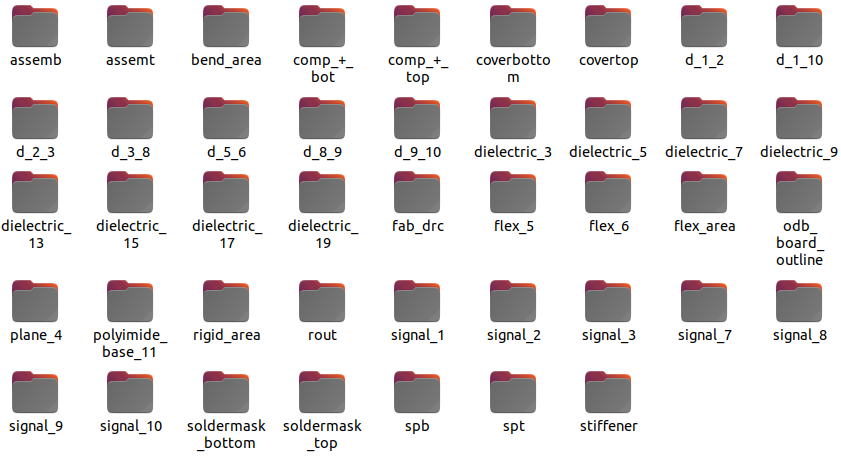
Sample section from a matrix file:
LAYER {
  ROW=4
  CONTEXT=BOARD
  TYPE=SIGNAL
  NAME=SIGNAL_1
  POLARITY=POSITIVE
  START_NAME=
  END_NAME=
  OLD_NAME=
  ADD_TYPE=
  COLOR=0
  ID=5
}
As per "Importing and Meshing a PCB Geometry from an ODB++ Archive" from COMSOL Inc: 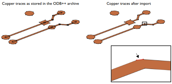
ODB++ and EMN/EMP, both are part of the Intermediate Data Format - IDF used to transfer PCB design data. EMN/EMP is an older simpler format primarily used for mechanical, 3D clearance checks between ECAD and MCAD tools ensuring boards fit inside mechanical enclosures. EMN/EMP lacks detailed electrical information and cannot be used for manufacturing. IDX (Incremental Data eXchange) as the name suggests, it is an XML-based format that lets import and export of incremental data into the design iterations cycle. Enables 'bidirectional' collaboration, allowing MCAD users to propose component position changes and ECAD users to accept or reject them.
IPC-2581 is a new standard from the IPC (International Printed Circuit association). ODB++ is often considered a competitor to IPC-2581 which is also a comprehensive manufacturing format. IPC-2581 is an open-standard, XML-based, vendor-neutral, and free alternative managed by a consortium. IPC-2581 generates a single XML file which is capable of including all information needed to fabricate and assemble the printed board assembly. One of the key reason for Gerber still being widely used format is that PCB manufacturers continue to use Gerbers for quoting and designers continue to share Gerbers to them."Electronic Schematics: Schematics communicate specific information about how electronics in a design should be connected to each other. Components are labelled with their electrical characteristics, such as capacitance or resistance, with the complete circuit being illustrated across the PCB. The schematic is an organized view of the electrical circuit and provides necessary information for manufacturing."
Typical *.emn File Entry
#------------------------------------------------------------------------------
#The comment character is the pound sign (#). A comment must be a separate line
#(record) and the comment character must be in column 1. Comments should be
#located between, but not within sections of the IDF files.
#------------------------------------------------------------------------------
.HEADER
BOARD_FILE 3.0 "Sample File Generator" 2020/07/01.16:02:44 1
sample_board THOU
.END_HEADER
#Unit MM or THOU = milli-inch
#------------------------------------------------------------------------------
#Section keyord: .BOARD_OUTLINE or .PANEL_OUTLINE
#MCAD - Outline is owned by the Mechanical system and should not be modified in
#the Electrical system
#ECAD - Outline is owned by the Electrical system and should not be modified in
#the Mechanical system
#UNOWNED - Outline can be modified in either system
#62.0 is thickness in milli-inch
#------------------------------------------------------------------------------
.BOARD_OUTLINE MCAD
62.0
0 5030.5 -120.0  0.0
0 5187.5 -120.0  0.0
0 5187.5  130.0  0.0
0 5155.0  130.0  0.0
0 5155.0  550.0 -180.0
...
.END_BOARD_OUTLINE
#------------------------------------------------------------------------------
.ELECTRICAL
EthnetBrd 135792468 THOU 59.0
0 -92.0  63.0 0
0 -92.0 -63.0 0
0  92.0 -63.0 0
0  92.0  63.0 0
0 -92.0  63.0 0
.END_ELECTRICAL
#------------------------------------------------------------------------------
EthnetBrd 135792468 E7
20.5 32.5 0.0 90.0 BOTTOM PLACED
- EthnetBrd is the ECAD name
- 135792468 is the ecad_alt_name (unique part number)
- E7 is the reference designator
- 20.5, 32.5 0.0 represent the location with respect to the origin of PCB (0,0) point X, Y, Z directions
- 90.0 represents the orientation of the component
- BOTTOM specifies the side of the PCB
- PLACED specifies component will be added to 3D PCB
These softwares are meant for electronics industry mainly and hence contains many built-in objects to expedite the simulation process. They can be summarized as follows:

- Primitive - Fundamental geometric entities in FloTHERM and ICEPAK: Cuboids, Prisms and Flow Resistances
- SmartPart - Object parametrically created out of Primitives: e.g. Enclosure, fan, PCB, cylinders, volume or surface heat source, heat sinks (described by base dimension, number of fins, fin width and fin height), perforated plate (fully designated by hole size and arrangement, pitch, free area ratio)
- Assembly - A group of Primitives, SmartParts and Sub-Assemblies
- Attribute - A property that can be attached to Primitives and SmartParts (e.g. material properties)
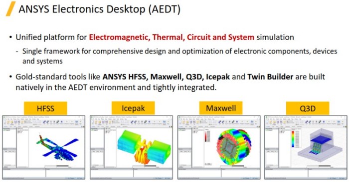
Primitives defined in ICEPAK
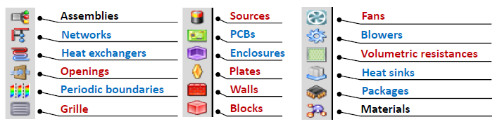
Reading Mechanical CAD (MCAD) data
- The MCAD data can be read either in their native format such as ProE, Solidworks or CATIA files (parts and assemblies) or neutral formats such as IGES, STEP or PARASOLID.
- After initial defeaturing (removal of chamfers and fillets) and simplifications (removal of small holes, branding logos, part identifiers), the MCAD geometry needs to be converted into ICEPAK / FloTHERM entities.
- Simplification is permissible to the to the extent where the geometry could be created manually using primitives and smart-parts in ICEPAK / FloTHERM!
- The conversion into ICEPAK / FloTHERM entities is a process of replacing a detailed geometry say perforated plate with a plate of same size without perforation and specifying the perforation details as attributes to the ICEPAK / FloTHERM entities.
Mesh generation process and recommendations
- For naturally convected cases, the computational domain needs to be made bigger than the chassis or the board.
- For the space above the chassis extend the domain 2~3 × height of chassis. Note that the buoyancy may not be strong enough to establish a flow from lower face to upper face and reverse flow can be observed on both of these faces. In order to reduce the reverse flows, the domain boundaries may need to be kept closer to the heat source.
- For space below chassis extend the domain equal to the height of chassis.
- For the remaining sides (front, rear, left and right) of the chassis, extend the domain 0.5 ~ 1.0 × depth and width of the chassis.
- In case on natural convection, the heat transfer through convection is low and hence radiation also contributed significantly. Up to 50% of heat transfer is by radiation and remaining 50% by natural convection.This can be justified by the fact that the HTC value for natural convection in air varies between 5~10 [W/m2.K] whereas equivalent HTC for radiative heat transfer = ε × σ × (TWALL4 - TAMB4) / (TWALL - TAMB) = 4.9 [W/m2.K] for ε = 0.5, TWALL = 100 [°C] and TAMB = 50 [°C].
- The components are mostly represented as volume with sharp corners such as cuboid and rectangles. A cut-cell method also known as trimmer mesh or Cartesian mesh or snappyHexMesh (in OpenFOAM) is used in ICEPAK and FloTHERM.
- For printed circuit boards as in any surface with a significant amount of heat flux, 3 cells in the first millimeter above the board (air volume) and 3 cells in the first millimeter below the board (solid volume) is recommended.
- Maintain aspect ratio of cells < 100.
- For fins, maintain > 5 cells cross a channel for better heat transfer and pressure drop prediction, use two or more cells across the thickness in the solid.
Special applications in Electronic Cooling
- Thermo-Electric Cooling (TEC): This device is based on Peltier effect where thermal energy is absorbed at one dissimilar metal junction and discharged at the other junction when electric current flows within a closed circuit. It comprises of p-type and n-type semiconductors sandwiched between ceramic electrical insulators. TEC are solid state heat pumps for applications where cooling below ambient are required. The cold junction acts as 'evaporator' and hot junction as 'condenser' of a refrigeration cycle.
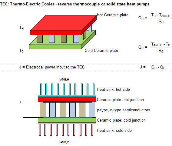
- Seebeck Effect: ΔV = α × (TH - TC) where α [V/K] = differential Seebeck coefficient or (thermo-electric power coefficient) between the two materials, positive when the direction of electric current is same as the direction of heat flow.
- QH [W] = β [V] × I [A] where β is differential Peltier coefficient between given two materials
- β < 0: Electric current and heat flow in opposite directions
- β > 0: Electric current and heat flow in same directions
- COP = coefficient of performance of the thermoelectric device = QC / J, which typically is between 0.4 and 0.7 for single stage applications.
- Heat Pipe: Capillary effect and phase change (evaporation and condensation) are the phenomena which define operation of heat pipes. Due to phase change from liquid to vapour, the heat transfer coefficient for heat pipes is extremely high - of the order of 40,000 [W/m2.K]. Originally invented by NASA for space application, it has gained widespread application in electronics industry.
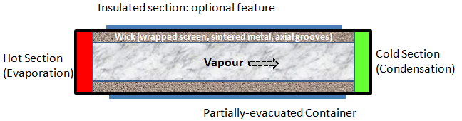
Schematic of heat pipe in rack cooling as per "Investigation on thermal design of a rack with the pulsating heat pipe for cooling CPUs", Applied Thermal Engineering, 110, 390– 398 by Dang et. al.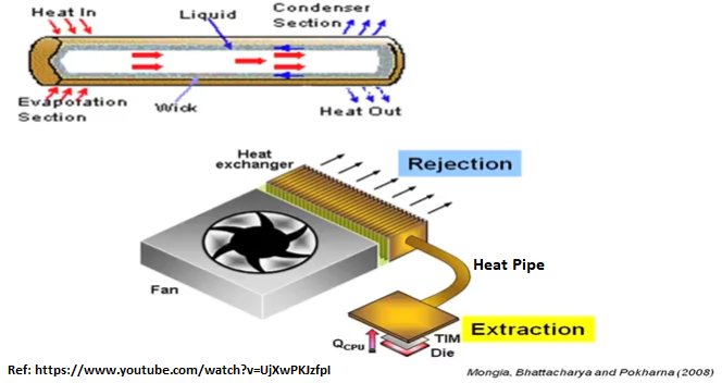
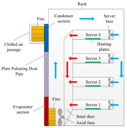
- Heat Spreader: This is an application similar to heat sink. The purpose of a heat spreader is to use material with a very high thermal conductivity such as graphite with k = 1400 [W/m-K] to make the heat flow in-plane over a larger area so that it can be further dissipated into ambient using heat sinks. Another variant is thermal strap which is a metallic but flexible connection between heat source and a sink usually the chassis wall or enclosure wall.
- Thermal Vias: These are thin (hollow or solid) pins acting as pathways in a PCB to transfer heat away from hot components to a cooler area such as heat sink or ground plane. Note vias are also used to connect electrical signals between layers of a PCB. Thermal vias are specifically designed to manage heat transfer path acting like heat spreader.
- Typical thickness of thermal vias is 0.3 [mm]
- They can be follow tube or filled with conductive epoxy or copper
- Filled vias are capped from both ends with copper to provide flat surface for soldering
- The centre-distance between two adjacent vias should be > 1.0 mm to prevent solder wicking
- Solder wicking is the phenomena where molten solder is drawn into the via by capillary action
- To prevent solder wicking, vias are filled with epoxy and covered with plate (via-in-pad)
- Large copper areas (like thermal pads) draw heat, pulling solder towards them
The effect of thermal vias on through-the-plane thermal conductivity can be estimated with this simple calculator.
PCM - Phase Change Material: These are energy storage and release mechanism based on change of phase (typically solidification and melting). The material can be used to keep temperature fluctuations low in case of heating and cooling cycles. Sometimes, the PCM can also act as an insulator to heat dissipation based on thermal conductivity. Some key characteristics required for a energy storage and release type PCM are tabulated below.
| Characteristics | Desired value | Remark |
| Melting point, TMP | As per temperature control | Selection of material will depend on temperature to be maintained |
| Specific heat capacity, Cp | High | Energy storage capacity ∝ Cp. Higher the Cp, lesser the mass required to store a given amount of energy. |
| Density, ρ | High | Energy storage capacity ∝ ρ and the volume required is also less as m = ρ * V |
| Thermal Conductivity, k | High for energy storage purpose | Low value is required for insulation where heat is to be maintained near the source itself |
| Coefficient of volume expansion, γ | Low | This governs flexibility or void space required in the storage container |
| Chemical compatibility | Non-corrosive | Should not react with the container and other materials in case of leaks |
| Thermal cycling (heating-cooling) stability | No degradation | The micro-structure and material properties should not degrade with heating-cooling cycles |
TEC Performance Calculation
Field Variables
- i = Current [A]
- k = Thermal conductivity of TEC block [W/m-K]
- QH = heat rejection from hot surface (the 'condenser') [W]
- QC = heat absorption by cold surface (the 'evaporator') [W]
- R = Electric Resistance of TEC assembly [Ω]
- TC = cold side temperature (the 'evaporator') [K]
- TH = hot side temperature (the 'condenser') [K]
- P = power consumption by TEC device = (QH - QL) [W]
- S = seebeck co-efficient [V/K]
- ΔT = temperature difference between hot and cold junction [K]
- G = Ratio of cross-section area to the length (thickness) of the device [m]
- ρ = resistivity of TEC device [Ω-m]
- COP = Coefficient of Performance = QC / P
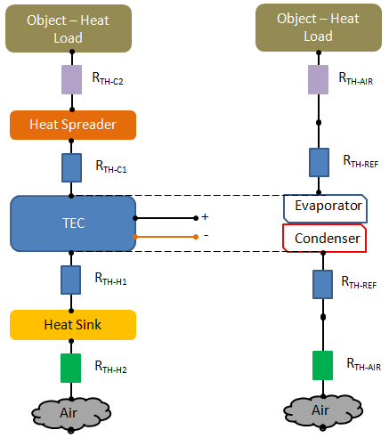
Or
QC = -[S.i.TC - 0.5 × i2ρ/G − k×G×(TH − TC)]
Similarly:
QH = [S.i.TH + 0.5 × i2R − k.×G×(TH − TC)]Or
QC = [S.i.TH + 0.5 × i2ρ/G − k×G×(TH − TC)]
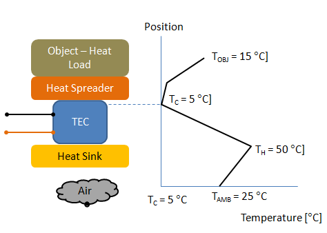
Anisotropic or Orthotropic Thermal Conductivity: The printed-circuit boards are formed by many layers of copper wires known as traces and dielectric material (say FR4). They are so thin that they cannot be modelled (meshed and boundary conditions applied) separately. Hence, the thermal conductivity of board can be simplified using equivalent uniformed value along the thickness and in-the-plane direction. This simplification is done using series and parallel arrangement of thermal resistances analogous to electrical resistances.
Orthotropic conductivity based on lumped block assumptions. 10% Copper is a reasonable guess. In case one needs to use "Locally Varying Orthotropic" thermal conductivity, the detail layout of traces and FR4 layers need to be modelled.
- kIN_PLANE = VFCu × kCu + (1-VFCu) × kDie
- 1/kX_PLANE = VFCu / kCu + (1-VFCu) / kDie
- Here, VF = Volume Fraction of copper in fractions (that is the value lies between 0 and 1).
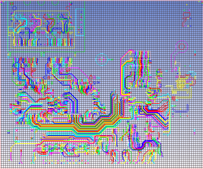
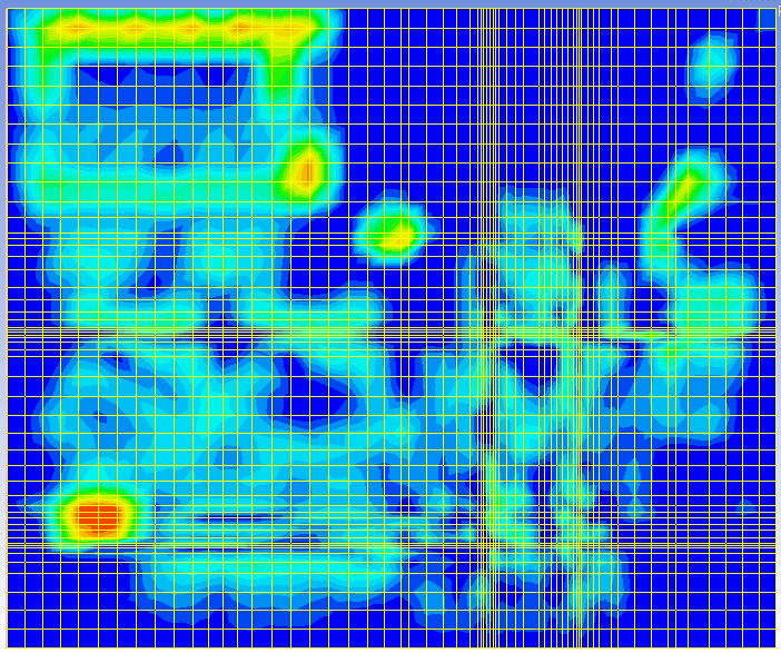
kLAYER_i = kCu × ACu / APCB + kFRP × AFRP / APCB
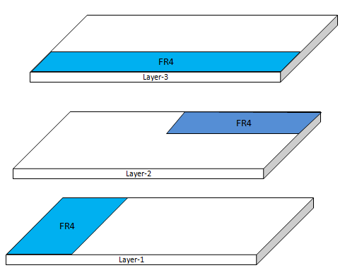
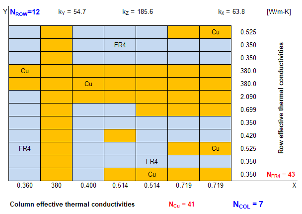
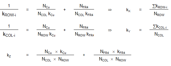
ICEPAK is a GUI for pre- and post-processing. It uses FLUENT as solver and in this process many files get created. Following is a list of files and its owner (ICEPAK or FLUENT?).
| File Type | Created by | Used by | Suffix / Filename | Remark |
| Model | ICEPAK | ICEPAK | model | |
| Problem | ICEPAK | ICEPAK | problem | |
| Job | ICEPAK | ICEPAK | job | |
| Mesh input | ICEPAK | mesher | grid_input | Inputs for the mesh generator. |
| Mesh output | mesher | ICEPAK | grid_output | Output from the mesh generator that is the mesh file |
| Case | ICEPAK | FLUENT | .cas | Contains all the information that is needed by ICEPAK to run the solver |
| Data | FLUENT | FLUENT | .dat and .fdat | Files when it has finished calculating: *.dat and *.fdat. These data files can be used to restart the solver |
| Residual | FLUENT | ICEPAK | .res | Information about convergence monitors: Solve → Solution monitor or select Convergence plot in Post menu |
| Script | ICEPAK | ICEPAK | .SCRIPT or _sc.bat | Runs the solver executable and can also be used to run the solver in batch mode. |
| Solver input | ICEPAK | FLUENT | .uns_in | The solver input file (projectname.uns_in) is read by the solver to start the calculation. |
| Solver output | FLUENT | – | .uns_out | Information from solver that is displayed on screen during calculation - this file is written only on Linux systems |
| Diagnostic | ICEPAK | – | .diag | Contains information about correspondence between object names in model file and object names in case file |
| Optimization | ICEPAK | optimizer | .log, .dat, .tab, .post, .rpt | Optimization of field variables |
| Postprocessing | FLUENT | ICEPAK | .resd | Used by ICEPAK for post-processing. All solutions that exist for the current project are listed by solution ID. |
| Log | ICEPAK | ICEPAK | .log | |
| Geometry | External | ICEPAK | .igs, .stp | CAD geometry - input to ICEPAK |
| Packaged | ICEPAK | ICEPAK | .tzr | Project archive |
Few keyboard short-cuts and special topics in ICEPAK
- Move legend with Ctrl and the middle mouse button
- Edit levels and set orientation with shift right-click on legend
- Move the cut-plane in the domain with shift and the middle mouse button
- Shift middle-click on CAD objects to graphically move the CAD geometry
- Thermal Chokepoint: the dot product of heat flux and temperature gradient - it shows regions of high heat flux experiencing large thermal resistances
- Thermal Cross: the cross product of heat flux and temperature gradient - it shows regions where large heat flux vectors not aligned with high thermal gradients
Thermal Simulations: Basic Solver Setting
Note that ICEPAK uses FLUENT in background as solver.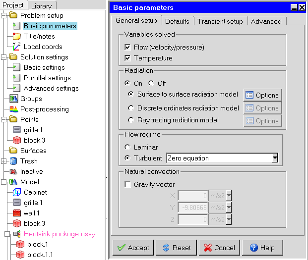
Mesh Generation
The default option in ICEPAK is to generate a Cartesian mesh similar to snappyHexMesh in OpenFOAM, trimmer mesh in STAR-CCM+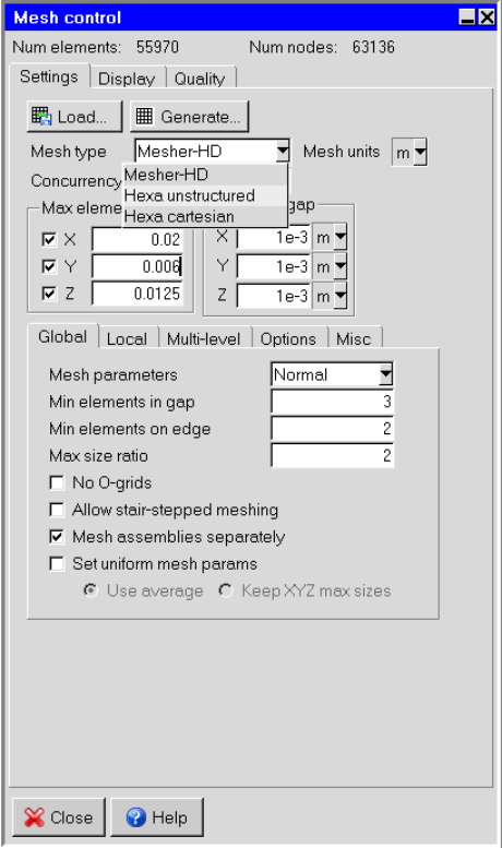
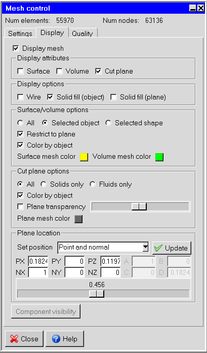
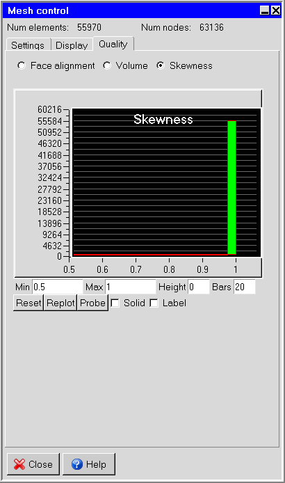
Fan, Fins and Grilles
There are many in-built feature to model flow resistances and momentum sources / sinks.
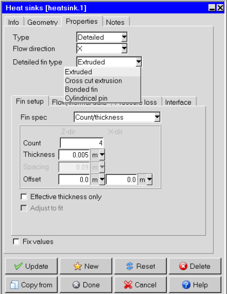
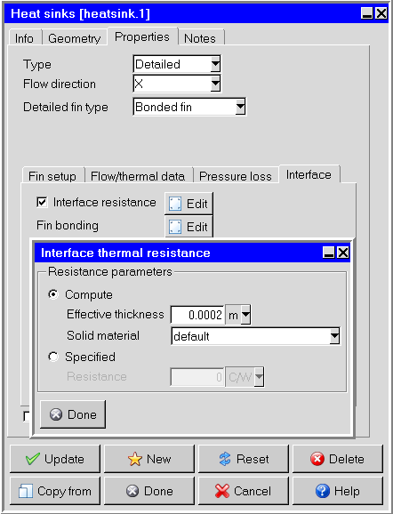
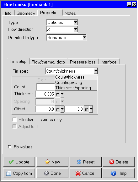
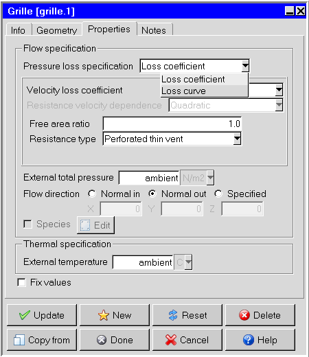
Boundary Conditions
Wall boundary condition: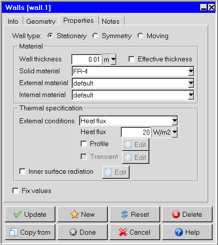
PCB Gerber or ODB++ File Import: Bring in an actual PCB primitive from the list. Open the PCB block by double-clicking on it or right-click and select Edit. Click on the Geometry tab, to Import the ECAD file (such as an ODB++ file).
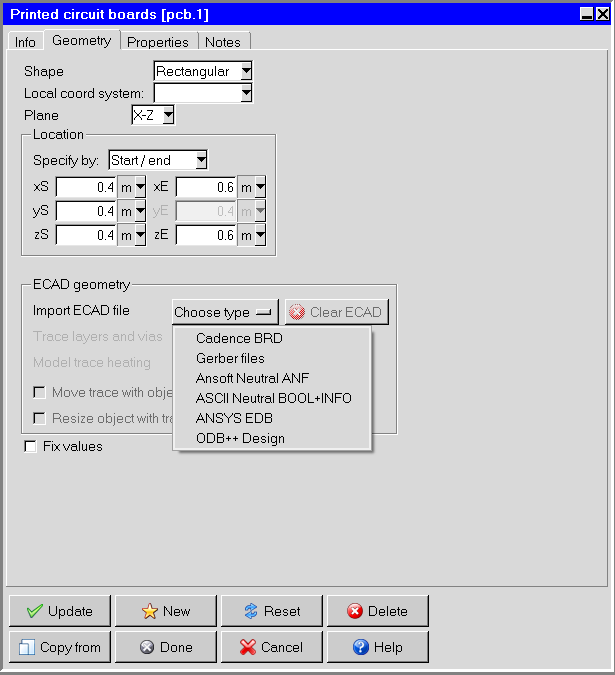
PCB Stack Data
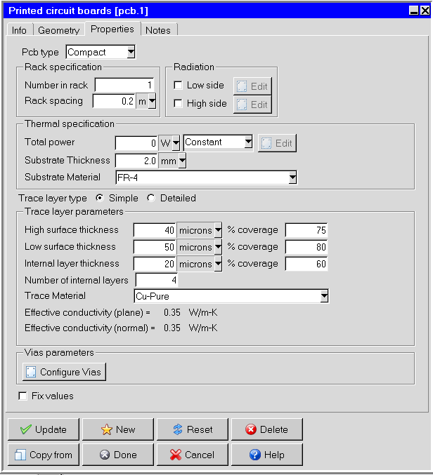
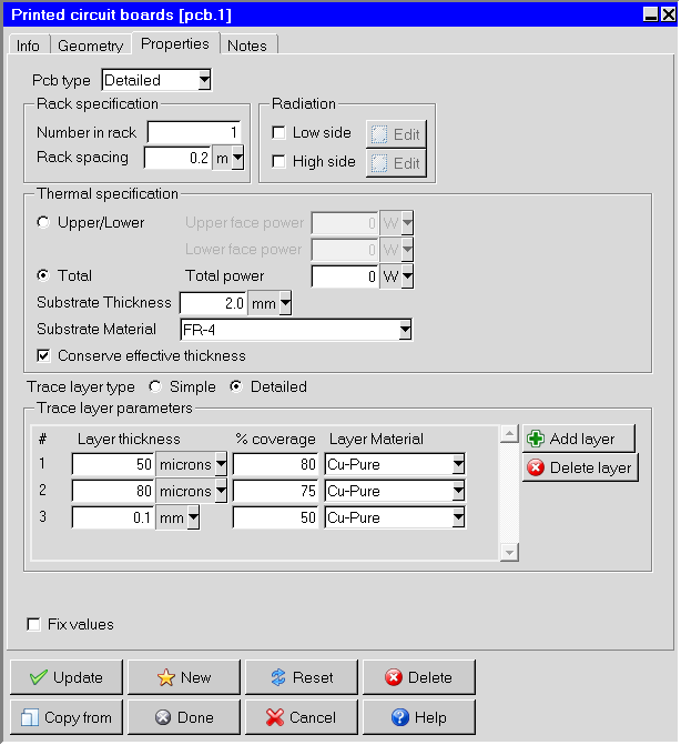
Monitors and Runs Settings
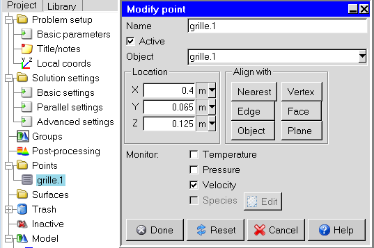
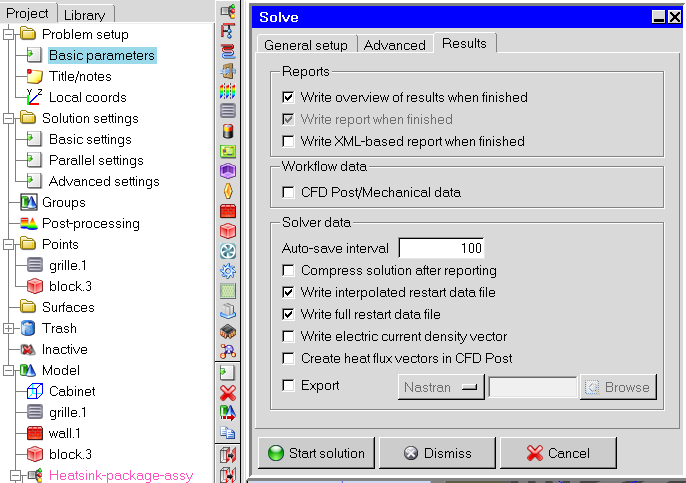
Micro-Channels
Cooling systems in the field of microelectronics and microelectromechanical systems (MEMS) use small and microscale flow passages. The transport phenomena in microscale channels are very different as compared to conventional size channels or macroscale channels. There are several dimensionless numbers used to represent the feature of fluid flow in microscale channels, similar to Reynolds number in macro-chnnels. The distinction between macro- and microscale channels may also be classified according to these dimensionless numbers.Heat Transfers from Extended Surfaces (Fins)
This section provides a way to calculate heat transfer rate and estimate typical range of values for designs. Two design criteria used to define performance of fins are "fin efficiency" and "fin effectiveness". Fin efficiency is ratio of "actual heat transferred through fins" to the "heat that would be transferred if the entire fin were as base temperature".Material Properties of Fins: as per technical brief "Heat Sink Design Facts & Guidelines for Thermal Analysis" by Wakefield-Vette,
| MATERIAL | CONDUCTIVITY | USAGE |
| (Series/Alloy) | k (W/m-K) | (Product Type) |
| Al-5052 H36 | 138 | Stampings |
| Al - 6061 T6 | 167 | Extrusions |
| Al - 6063 T6 | 209 | Extrusions |
| Al - 1100 H14 | 220 | Stampings |
| Cu - CDA110 | 300 | Bonded-Fin |
| Cu - CDA101 | 398 | Heat Spreaders |
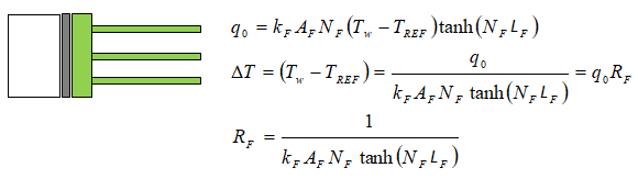
Such fins are extruded or machined and needs to be fixed on the heat generating component using adhesive or screws. This creates a thermal contact resistance and needs to be accounted for temperature calculation of the mating surfaces. The parameter ΔT/[Q.A] can be used in fin selection for given heat dissipation and surface area (available space). Lower the number, better the heat sink design.
| BF | Thickness of fins | [mm] | 1 | 2 | 2 | 2 | 5 | 5 |
| LF | Height of fins | [mm] | 20 | 20 | 10 | 20 | 20 | 10 |
| WF | Width of fins [depth perpendicular to screen] | [mm] | 250 | 250 | 250 | 250 | 100 | 100 |
| AF | Cross-section of fins = BF×WF | [mm2] | 250 | 500 | 500 | 500 | 500 | 500 |
| PF | Perimeter of fins = 2[BF+WF] | [mm] | 502 | 504 | 504 | 504 | 210 | 210 |
| kF | Thermal conductivity of fin | [W/m-K] | 100 | 100 | 100 | 100 | 100 | 100 |
| h | Convective Heat Transfer Coefficient | [W/m2-K] | 10 | 10 | 20 | 10 | 10 | 10 |
| NF | Fin parameter | [m-1] | 14.17 | 10.04 | 14.20 | 10.04 | 6.48 | 6.48 |
| RF | Thermal resistance of each fin | [K/W] | 10.23 | 10.05 | 9.99 | 10.05 | 23.94 | 47.69 |
| iF | Number of fins | [nos] | 10 | 10 | 10 | 10 | 10 | 10 |
| RF | Thermal resistance of all fins | [K/W] | 1.02 | 1.01 | 0.99 | 1.01 | 2.39 | 4.77 |
| ΔT | Temperature potential | [K] | 60 | 60 | 60 | 60 | 60 | 60 |
| Q | Heat transfer rate (all fins) | [W] | 58.7 | 59.7 | 60.1 | 59.7 | 25.1 | 12.6 |
| A | Heat transfer surface area | [cm2] | 10 | 10 | 5 | 10 | 4 | 2 |
| ΔT/[A.Q] | Heat transfer rate | [K/W/cm2] | 0.102 | 0.101 | 0.200 | 0.101 | 0.599 | 2.384 |
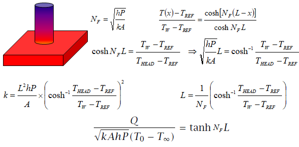
| Select the type of Fin: | |
| Thermal conductivity of fin in [W/m-K]: | |
| Specify length or height of fin [mm]: | |
| Diameter (pin-type) or thickness (plate-type) of fin [mm]: | |
| Width of plate-type fin [mm]: | |
| Convective HTC on fin surface [W/m2.K]: | |
| Reference temperature [°C]: | |
| Base temperature [°C]: | |
| Base thickness [mm]: | |
| Tip convection [W/m2.K]: | |
The heat transfer rate of pin-type fin for natural convection in air is tabulated below. Note the impact of L/D ratio on heat transfer rate.
| L | [mm] | 100.0 | 100.0 | 100.0 | 100.0 | 100.0 | 100.0 | 100.0 |
| D | [mm] | 5.0 | 10.0 | 20.0 | 25.0 | 50.0 | 100.0 | 200.0 |
| h | [W/m2-K] | 10.0 | 10.0 | 10.0 | 10.0 | 10.0 | 10.0 | 10.0 |
| ΔT | [K] | 60.0 | 60.0 | 60.0 | 60.0 | 60.0 | 60.0 | 60.0 |
| NF | [m-1] | 8.9 | 6.3 | 4.5 | 4.0 | 2.8 | 2.0 | 1.40 |
| A | [cm2] | 15.7 | 31.4 | 62.8 | 78.5 | 157.1 | 314.2 | 628.3 |
| Q | [W] | 0.7520 | 1.6680 | 3.5370 | 4.4760 | 9.18 | 18.60 | 37.45 |
| ΔT/[A.Q] | [K/W/cm2] | 5.079 | 1.145 | 0.270 | 0.1707 | 0.0416 | 0.0103 | 0.0025 |
The values for forced convection in air is tabulated below. 'A' is the heat transfer area of the fin and not the cross-section area. The parameter ΔT/[Q.A] can be used in fin selection for given heat dissipation and surface area (available space). For example, for a heat dissipation of 10 [W] using a fin of diameter 20 [mm] and height 100 [mm], the expected increase in temperature of the base of fin is 10 [W] x 62.8 [cm2] x 0.1431 = 89.9 [K].
| L | [mm] | 100.0 | 100.0 | 100.0 | 100.0 | 100.0 | 100.0 | 100.0 |
| D | [mm] | 5.0 | 10.0 | 20.0 | 25.0 | 50.0 | 100.0 | 200.0 |
| h | [W/m2-K] | 20.0 | 20.0 | 20.0 | 20.0 | 20.0 | 20.0 | 20.0 |
| ΔT | [K] | 60.0 | 60.0 | 60.0 | 60.0 | 60.0 | 60.0 | 60.0 |
| NF | [m] | 8.9 | 6.3 | 4.5 | 4.0 | 2.8 | 2.0 | 1.40 |
| A | [cm2] | 15.7 | 31.4 | 62.8 | 78.5 | 157.1 | 314.2 | 628.3 |
| Q | [W] | 1.270 | 3.008 | 6.673 | 8.533 | 17.905 | 36.725 | 74.409 |
| ΔT/[A.Q] | [K/W/cm2] | 3.0070 | 0.6350 | 0.1431 | 0.0895 | 0.0213 | 0.0052 | 0.0013 |
The chart below provides a comparison between two designs of circular fins. Here, L ≡ r2 - r1 and 'A' is based on section shaded in dark colour. Reference: A Textbook of Heat Transfer by Lienhard and Lienhard.
More on LED
Thermal Resistances
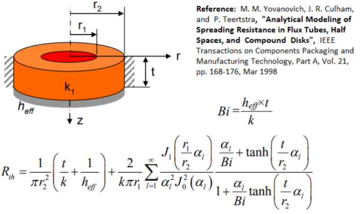
Thermal Simulations in Data Centres
The simulations of data centres can be grouped into sub-systems and multi-scale models. The super-system is the room itself followed by systems such as racks and plenum/ducting following by sub-systems like servers, server-mounted heat exchangers, appliances, mechanical systems (fans, blowers, dehumidifiers), cold-plates, and even Insulated-Gate Bipolar Transistor (IGBT). The simulation gets further complicated by change in weather conditions during the day and over a longer time periods.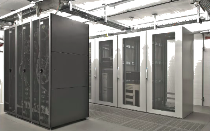
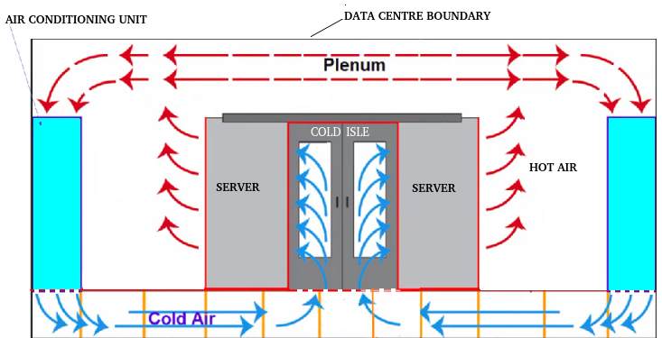
The content on CFDyna.com is being constantly refined and improvised with on-the-job experience, testing, and training. Examples might be simplified to improve insight into the physics and basic understanding. Linked pages, articles, references, and examples are constantly reviewed to reduce errors, but we cannot warrant full correctness of all content.
Template by OS Templates